
Introduction to Amplifier
Amplification is the process of increasing the amplitude of a AC signal current or voltage such as audio signal for sound or video signal for a television picture. The amplifier allows a small input signal to control a larger amount of power in the output circuit. The output signal is a copy of the original input signal but has higher amplitude.
Amplification is neccessary as in most applications, the signal is too weak to be used directly. For example, an audio output of 1mV from a microphone is not able to drive a loud speaker which requires a few volts to operate. Hence, the signal need to be amplified to a few volts before it can be fed into the loud speaker.
NPN Transistor Circuit Configurations
An example of different type of transistor configurations in the circuit is as shown in Figure 1 below.
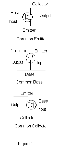
b) The common base (CB) circuit uses base as its common electrode. The input signal is applied to the emitter and the amplified output is taken from the collector. The relatively high emitter current compared to the base current results in very low input impedance value. For this reason, the CB circuit is seldom used.
c) The common collector (CC) circuit uses collector as its common electrode. The input signal is applied to the base and the amplified output is taken from the emitter. This circuit is also called an emitter follower. This name means that the output signal voltage at the emitter follows the input signal at the base with the same phase but less amplitude. The voltage gain is less than 1 and is usually used for impedance matching. It has high input at the base as a load for the preceding circuit and low output impedance at the emitter as a signal source for the next circuit.
Classes
They can be classified into classes A, B, C and AB. They are defined based on the percent of the cycle of input signal that is able to produce output current.
In Class A, the output current flows for the full cycle of 360 degree of input signal. The distortion is the lowest with around 5% to 10% and an efficiency of 20% to 40%. In general, most small signal operate class A
In Class C, the output current flows for less than one half of the input cycle. Typical operation is 120 degree of input current during the positive half cycle of the input current. This class has an efficiency of 80% but has the highest distorton. This class is usually used for RF amplificaton with a tuned circuit in the output.
In Class B, the output current flows for one half of the input cycle which is around 180 degree. Class B operaton lies between class A and class C. Clas B are usually connected in pairs and in such a circuit called push-pull amplifier. The push-pull is often used for audio power output to a loud speaker.
In Class AB, it offers a compromise between the low distortion of class A and the higher power of class B. It is usually used for push-pull audio power amplifiers.
1 W Home Stereo Amplifier Project
Introduction To Home Stereo Amplifer
This is a 1 watt home stereo amplifier module project using the KA2209 IC from Samsung, which is equivalent to the TDA2822. It operates from 3-12V DC and will work from a battery since the quiescent current drain is low. It requires no heat sink for normal use. The input and output are both ground referenced. Maximum output will be obtained with a 12V power supply and 8 ohm speaker, however it is particularly suitable for driving headphones from a supply as low as 3V.
The Specifications of the home stereo amplifier are:
D.C. input : 3 – 12 V at 200 – 500 mA max
Idle current : approx. 10 mA
Power output : > 1 Watt max. 4-8 ohms, 12V DC
Freq. Resp. : approx. 40 Hz to 200 kHz, 8 ohm, G=10
THD : <> 80 dB, G = 20 dB
Sensitivity : < g =" 20">
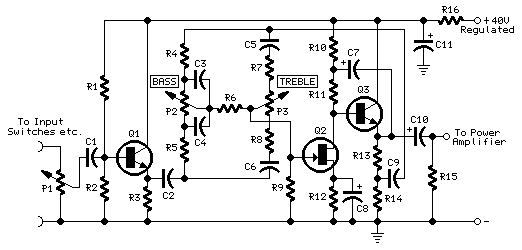
Home Stereo Amplifier Description

This will keep the signal to noise ratio as high as possible. Extra gain provided by the amplifier will reduce the S/N ratio by a similar amount, since the input noise figure is constant. Other values for R1 and R3 of between 1k and 10k ohm can be used if an intermediate gain level is required.
Voltage Gain = 1+ R1/R2 = 1+R3/R4, however the maximum gain with no external feedback is approximately 100, or 40dB. (GdB = 20log Gv)
If driving a pair of headphones, you may also require a 100 ohm resistor in series with each output to reduce the output level, depending on headphone impedance and sensitivity. Make sure you start with the volume right down to check. A number of headphones may be driven from the one amplifier if you wish, since most headphones have at least 16 ohm impedance, or more commonly 32 ohm.
There are only a few external components, the IC contains most of the necessary circuitry. R1,R2 and R3,R4 are the feedback resistors. C1 provides power supply decoupling. C2 and C3 are the input coupling capacitors, which block any DC that might be present on the inputs. C4,C5 block DC in the feed back circuit from the inverting inputs, and C6,C7 are the output coupling capacitors. C8, R5 and C9,R6 act as zobel networks providing a high frequency load to maintain stability at frequencies where loud speaker inductive reactance may become excessive. The pot provides adjustable input level attenuation.
Home Stereo Amplifier Parts List

You may download the full data sheet for the
18W Car Stereo Amplifier Using HA13118 IC
Introduction To 18W Car Stereo Amplifier Project
This car stereo amplifier project is a class AB audio power amplifier using the Hitachi HA13118 module. It not only can be used in car application but also in any portable or home amplifier system. It is easy to construct and has a minimum of external components. The module has a high power output from a low voltage supply using the bridge tied load method, and a high gain of 55dB.
This project will be especially useful in applications where the input signal is a low level, without requiring the use of a separate pre-amplifier. This IC module has a built in surge protection circuit, thermal shut down circuit, ground fault protection circuit and power supply fault protection circuit making it extremely reliable.
The Specifications of this project are:
D.C. Input : 8 – 18V at 1-2 A
Power output : 18W maximum, 4 ohm load, 18V DC supply
S/N ratio : > 70 dB
THD : <>
Freq. Response : ~ 30 Hz to 30 kHz, –3 dB
Input level : <> 50dB)
Input Impedance : ~ 30 k ohm
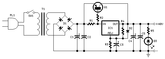
The supply voltage required for this project is 8 -18V DC, at least 1 to 2 Amps. Maximum output power will only be obtained with a power supply of 18V at greater than 2 A, using a 4 ohm speaker. The power supply should be well filtered to reduce mains hum, a regulated supply will reduce noise even further. Extra filtering is unnecessary if operating from a battery supply.
Circuit Diagram Description

An externally mounted logarithmic potentiometer of between 10k ohm and 50k ohm, is used depending on the desired input impedance. The impedance should be keep as high as possible for a guitar amp, unless using a separate pre-amp. Make sure that the heat sink is mounted to the module.
Parts List

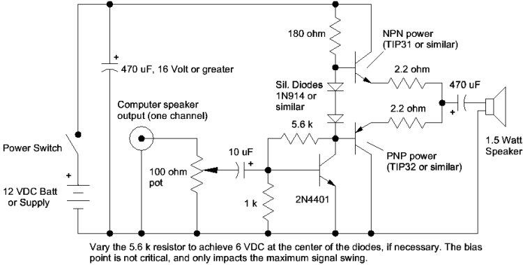
2. Computer Audio Booster
Here is a simple amplifier for boosting the audio level from low-power sound cards or other audio sources driving small speakers like toys or small transistor radios. The circuit will deliver about 2 watts as shown. The parts are not critical and substitutions will usually work. The two 2.2 ohm resistors may be replaced with one 3.9 ohm resistor in either emitter.
4-Transistor Amplifier for Small Speaker Applications
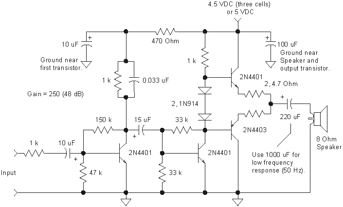
The circuit above shows a 4-transistor utility amplifier suitable for a variety of projects including receivers, intercoms, microphones, telephone pick-up coils, and general audio monitoring. The amplifier has a power isolation circuit and bandwidth limiting to reduce oscillations and "motorboating". The values are not particularly critical and modest deviations from the indicated values will not significantly degrade the performance.
Three cell battery packs giving about 4.5 volts are recommended for most transformerless audio amplifiers driving small 8 ohm speakers. The battery life will be considerably longer than a 9 volt rectangular battery and the cell resistance will remain lower over the life of the battery resulting in less distortion and stability problems.
The amplifier may be modified to work with a 9 volt battery if desired by moving the output transistors' bias point. Lowering the 33k resistor connected from the second transistor's base to ground to about 10k will move the voltage on the output electrolytic capacitor to about 1/2 the supply voltage. This bias change gives more signal swing before clipping occurs and this change is not necessary if the volume is adequate.
As before, the two 4.7 ohm resistors may be replaced with a single 10 ohm resistor in series with either emitter.
Op-Amp Audio Amplifier
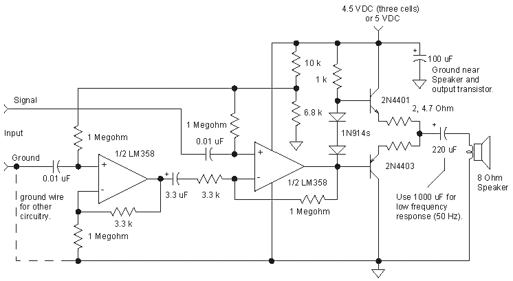
The above circuit is a versatile audio amplifier employing a low cost LM358 op-amp. The differential inputs give the amplifier excellent immunity to common-mode signals which are a common cause of amplifier instability. The dotted ground connection represents the wiring in a typical project illustrating how the ground sensing input can be connected to the ground at the source of the audio instead of at the amplifier where high currents are present. If the source is a power supply referenced signal then one of the amplifier inputs is connected to the positive supply. For example, an NPN common-emitter preamplifier may be added for very high gain and by connecting the differential inputs across the collector resistor instead of from collector to ground, destabilizing feedback via the power supply is greatly reduced.
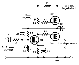
45 Watt Class B Amplifier
45W into 8 Ohm - 69W into 4 Ohm
Easy to build - No setup required
Circuit diagram:
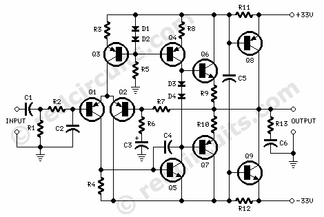
Parts:
R1______________18K 1/4W
Resistor R2_______________3K9 1/4W
Resistor R3,R6____________1K 1/4W
Resistors R4_______________2K2 1/4W
Resistor R5______________15K 1/4W
Resistor R7______________22K 1/4W
Resistor R8_____________330R 1/4W
Resistor R9,R10__________10R 1/4W
Resistors R11,R12_________47R 1/4W
Resistors R13_____________10R 1W
Resistor C1_______________1µF 63V
Polyester Capacitor C2_____________470pF 63V
Polystyrene or Ceramic Capacitor C3______________47µF 25V
Electrolytic Capacitor C4______________15pF 63V
Polystyrene or Ceramic Capacitor C6_____________220nF 100V
Polyester Capacitor C6_____________100nF 63V
Polyester Capacitor D1,D2,D3,D4___1N4148 75V 150mA
Diodes Q1,Q2________BC560C 45V 100mA
Low noise High gain PNP Transistors Q3,Q4________BC556 65V 100mA
PNP Transistors Q5___________BC546 65V 100mA
NPN Transistor Q6___________BD139 80V 1.5A
NPN Transistor Q7___________BD140 80V 1.5A
PNP Transistor Q8__________2N3055 60V 15A
NPN Transistor Q9__________MJ2955 60V 15A PNP Transistor
Power supply circuit diagram:
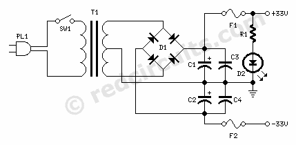
Parts:
R1_______________3K3 1/2W Resistor C1,C2_________4700µF 50V
Electrolytic Capacitors C3,C4__________100nF 63V Polyester Capacitors D1_____________200V 8A
Diode bridge D2_____________5mm. Red LED F1,F2__________4A Fuses with sockets
T1_____________230V or 115V Primary, 25+25V Secondary 120VA Mains transformer
PL1____________Male Mains plug SW1____________SPST Mains switch
Comments:
The main design targets for this amplifier were as follows:
- Output power in the 40 - 70W range
- Simple circuitry
- Easy to locate, low cost components
- Rugged performance
- No setup
These goals were achieved by using a discrete-components op-amp driving a BJT complementary common-emitter output stage into Class B operation. In this way, for small output currents, the output transistors are turned off, and the op-amp provides all of the output current. At higher output currents, the power transistors conduct, and the contribution of the op-amp is limited to approximately 0.7/R11. The quiescent current of the op-amp biases the external transistors, and hence greatly reduces the range of crossover.
The idea sprang up from a letter published on Wireless World, December 1982, page 65 written by N. M. Allinson, then at the University of Keele, Staffordshire.
In this letter, op-amp ICs were intended as drivers but, as supply voltages up to +/- 35V are required for an amplifier of about 50W, the use of an op-amp made of discrete-components was then considered and the choice proved rewarding.
The discrete-components op-amp is based on a Douglas Self design. Nevertheless, his circuit featured quite obviously a Class A output stage. As for proper operation of this amplifier a Class B output stage op-amp is required, the original circuit was modified accordingly.
Using a mains transformer with a secondary winding rated at the common value of 25 + 25V (or 24 + 24V) and 100/120VA power, two amplifiers can be driven at 45W and 69W output power into 8 and 4 Ohms respectively, with very low distortion (less than 0.01% @ 1kHz and 20W into 8 Ohms).
This simple, straightforward but rugged circuit, though intended for any high quality audio application and, above all, to complete the recently started series of articles forming theModular Preamplifier Control Center, is also well suited to make a very good Guitar or Bass amplifier. Enjoy!
Notes:
- 2N3055 and MJ2955 transistors were listed for Q8 and Q9 as the preferred types, but many different output transistors can be used satisfactorily: TIP3055/TIP2955, TIP35/TIP36, MJ802/MJ4502 amongst others.
- Discrete op-amp output transistors Q6 and Q7 do not require any heatsink as their cases remain at ambient temperature. Power transistors Q8 and Q9 should be mounted on a black, finned heatsink as usual.
Technical data:
- Output power (1KHz sinewave):
- 45 Watt RMS into 8 Ohms - 69W RMS into 4 Ohms
- Sensitivity:
- 0.81V RMS input for 45W output
- Frequency response @ 1W RMS:
- 15Hz to 23KHz -0.2dB
- Total harmonic distortion @ 1KHz:
- 1W 0.008% 20W 0.008% 45W 0.016%
- Total harmonic distortion @10KHz:
- 1W 0.01% 20W 0.015% 45W 0.025%
- Unconditionally stable on capacitive loads
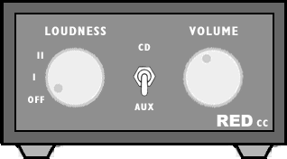
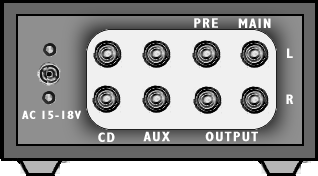
Modular Preamplifier Control Center
Volume and Loudness controls
CD and Aux inputs
Circuit diagram:
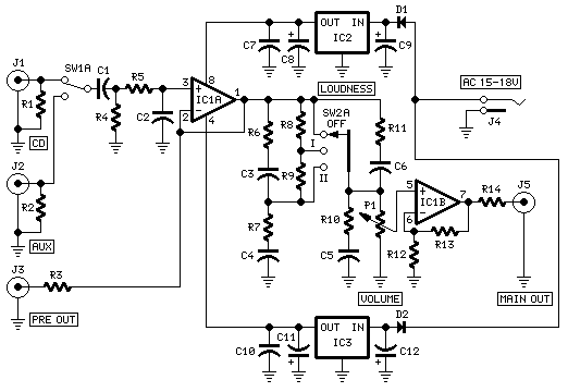
Parts:
P1______________47K Log. Potentiometer
(twin concentric-spindle dual gang for stereo) R1,R2,R4_______100K 1/4W
Resistors R3,R14_________560R 1/4W Resistors R5_______________1K 1/4W
Resistor R6,R7,R10_______10K 1/4W Resistors R8,R9___________22K 1/4W
Resistors R11_____________68K 1/4W Resistor R12______________1K5 1/4W
Resistor R13_____________12K 1/4W Resistor C1_______________1µF 63V
Polyester Capacitor C2,C3__________100pF 63V Polystyrene or Ceramic Capacitors
C4______________47nF 63V Polyester Capacitor C5______________22nF 63V
Polyester Capacitor C6_____________220pF 63V Polystyrene or Ceramic
Capacitor C7,C10_________100nF 63V Polyester Capacitors C8,C11___________4µ7 25V
Electrolytic Capacitors C9,C12________2200µF 25V Electrolytic Capacitors
IC1___________TL072 Dual BIFET Op-Amp IC2___________78L15 15V 100mA Positive
Regulator IC IC3___________79L15 15V 100mA Negative Regulator IC D1,D2________1N4002 200V 1A
Diodes SW1____________DPDT Toggle Switch SW2____________2 poles 3 ways
Rotary Switch J1,J2,J3,J5____RCA audio input sockets J4_____________Mini DC Power Socket
Comments:
This is the first article of a five-part series describing a complete audio preamplifier formed by five Mini-Modules, namely: Control Center, Switching Center, Phono Preamplifier, Tone Control and Headphone Amplifier. A suitable Power Amplifier module is already available here: 45 Watt Class B Amplifier.
The arrangement of these modules is similar to a late-1980's commercial production, the Thorens Restek Mini-Modules. Obviously, all the circuits of this Modular Preamplifier are original designs and have no relationship with the Thorens Modules.The modular arrangement allows the amateur to choose only the modules more suited to his requirements in order to build a chain one to five modules long.
For the minimalist, the Control Center module described in this page will be most probably the only useful module, allowing the choice of two input sources, e.g. a CD player and an Aux input (Tuner or iPod etc.).
The purist can also omit the Loudness control available there: the 2 poles 3 ways Rotary Switch used for this control (SW2) can be converted into a three-input selector switch. Therefore, the two-input selector SW1 at the center of the front panel, can be substituted by a 3mm stereo mini-jack socket, allowing, for example, the quick and easy plugging of an iPod.Each module, excepting the Switching Center that is a passive circuit, incorporates its own separate power supply rectifiers and regulators and requires only an external 15 - 18V ac (50mA minimum) Power Supply Adaptor.
In a chain formed by several modules, the use of a series of Power Supply Adaptors may be considered excessive. In such cases, the dual ±15V dc stabilized supply can be carried from a main module to the others by means of a three-wire cable and suitable connectors. Or the ac output of a single Power Supply Adaptor can be routed to several modules by using two Mini DC Power Sockets in each module wired in parallel, allowing to use a two-wire cable interconnection.Each electronic board can be fitted in a standard enclosure: Hammond extruded aluminum cases are well suited to host the boards of this preamp. In particular, the cases sized 16 x 10.3 x 5.3 cm or 22 x 10.3 x 5.3 cm are the more appropriate and can be stacked with advantage.
Control Center circuit description:
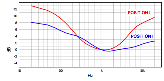
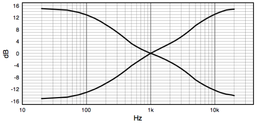
This circuit features two high-level inputs switched by SW1, followed by the unity-gain high input impedance buffer IC1A. The output of this buffer drives the passive network Loudness circuit. Its control switch SW2A allows the choice of two different frequency compensation curves (see graph below) to be used when the sound programme is reproduced at low levels. Curve I should be used with low to mid reproduction levels, in practice when the volume control knob is set around the second quarter of its travel. Curve II is best suited to very low levels, i.e. when the volume control knob is set around the first quarter. To obtain a perfectly flat frequency response, the Loudness control must be set in the OFF position.
The following Op-Amp (IC1B) provides all the gain required by the preamplifier, featuring 166mV RMS input sensitivity at 1.5V RMS output with very low distortion. Therefore it is capable of driving low input sensitivity power amplifiers.
The dual rail power supply necessary for this circuit is drawn from the single 15 - 18V ac voltage provided by a suitable external Power Supply Adaptor. D1 and D2 rectify respectively the positive and the negative half wave in order to obtain a dual opposite polarity rail voltage referred to ground. IC2 and IC3 provide a well regulated ±15V dc supply to the Op-Amps.
Notes:
- The circuit diagram shows the Left channel only and the power supply.
- Some parts are in common to both channels and must not be doubled. These parts are: P1 (if a twin concentric-spindle dual gang potentiometer is used), IC2, IC3, C7, C8, C9, C10, C11, C12, D1, D2, SW1, SW2 and J4.
- This module requires an external 15 - 18V ac (50mA minimum) Power Supply Adaptor.
Technical data:
- Input sensitivity:
- 166mV RMS for 1.5V RMS output
- Maximum output voltage:
- 9.5V RMS into 10K load
- Frequency response:
- flat from 20Hz to 23KHz
- Total harmonic distortion @ 1KHz and 10KHz:
- less than 0.002% at all levels up to 9.5V RMS (0.0017% typical)
Loudness Frequency Response:
A possible arrangement of the front and rear panels of this Module
Modular Preamplifier Tone Control
Bass and Treble Controls
Traditional or shelving frequency adjustment
Circuit diagram:

Parts:
P1,P2___________10K Linear Potentiometers
(twin concentric-spindle dual gang for stereo) R1_____________100K 1/4W
Resistor R2,R6___________18K 1/4W Resistors R3_______________3K3 1/4W
Resistor (18K for shelving curves: see Notes) R4,R5____________1K8 1/4W
Resistors (10K for shelving curves: see Notes) R7_____________560R 1/4W
Resistor C1_______________1µF 63V Polyester Capacitor C2_______________4n7 63V
Polyester Capacitor (3n3 for shelving curves: see Notes) C3_______________1µ5 63V
Polyester Capacitor (100nF for shelving curves: see Notes) C4,C7__________100nF 63V
Polyester Capacitors C5,C8___________22µF 25V Electrolytic
apacitors C6,C9_________2200µF 25V Electrolytic Capacitors IC1___________TL072
Dual BIFET Op-Amp IC2___________78L15 15V 100mA Positive Regulator IC IC3___________79L15
15V 100mA Negative Regulator IC D1,D2________1N4002 200V 1A Diodes SW1____________DPST
Toggle Switch J1,J2__________RCA audio input sockets J3_____________Mini DC Power Socket
Comments:
Needing a Tone Control, this module can be inserted in the chain between the Control Center and the Power Amplifier.
The circuit is based on an original design of Reg Williamson, published on Electronics World + Wireless World, Circuit Ideas, January 1991.This tone control circuit will take the form of either the traditional bass and treble adjustment or the shelving type, which is similar to a "tilt" control but with independent bass and treble.
Asymptotic slopes for both are about 4dB/octave, but begin to flatten out at 100Hz and 10kHz, reaching a maximum of ±15dB at the ends of the audio band.
Component values in parenthesis are those for the shelving type of control. In this case, the shelf begins at about 250Hz and 4kHz, flattening to a ±6dB maximum an octave above or below; the central point is 1kHz.
Reactive elements for the low end include a generalized impedance converter, which simulates an inductor in series with a resistor (gyrator).When set to the electrical centers of their respective controls, the reactive elements of the equalizers are virtually out of circuit. With these settings, the circuit behaves as a unity gain amplifier with 100% negative feedback. Even so, reactive elements can be switched out altogether with a DPST on/off switch.
As with the other modules of this series, each electronic board can be fitted into a standard enclosure: Hammond extruded aluminum cases are well suited to host the boards of this preamp. In particular, the cases sized 16 x 10.3 x 5.3 cm or 22 x 10.3 x 5.3 cm have a very good look when stacked. See below an example of the possible arrangement of the front and rear panels of this module.
Notes:
- To build the shelving type of control, use the values shown in parenthesis for R3, R4, R5, C2 and C3
- The circuit diagram shows the Left channel only and the power supply.
- Some parts are in common to both channels and must not be doubled. These parts are: P1 and P2 (if twin concentric-spindle dual gang potentiometers are used), IC2, IC3, C4, C5, C6, C7, C8, C9, D1, D2 and J3.
- This module requires an external 15 - 18V ac (50mA minimum) Power Supply Adaptor.
Technical data:
- Input sensitivity:
- 1V RMS for 1V RMS output
- Maximum output voltage:
- 9.5V RMS into 10K load
- Frequency response:
- flat from 20Hz to 23KHz
- Total harmonic distortion @ 1.5V RMS output:
- 100Hz = 0.004% 1KHz = 0.004% 10KHz = 0.002%
- Total harmonic distortion @ 6V RMS output:
- 100Hz = 0.003% 1KHz = 0.003% 10KHz = 0.03%
Traditional Bass and Treble Frequency Response:
Shelving Bass and Treble Frequency Response:

Mini-MosFet Audio Amplifier
Including Preamp, Tone Controls, Regulated dc Power Supply
18 Watt into 8 Ohm - 30W into 4 Ohm loads
Power Amplifier Circuit diagram:
Power Amplifier Parts:
R1_______________2K2 1/4W Resistor R2______________27K 1/4W Resistor R3,R4____________2K2 1/2W
Trimmers Cermet or Carbon (or 2K) R5_____________100R 1/4W Resistor R6_______________1K 1/4W
Resistor R7,R8__________330R 1/4W Resistors C1______________22µF 25V Electrolytic
Capacitor C2______________47pF 63V Polystyrene or Ceramic Capacitor C3,C4__________100µF 50V
Electrolytic Capacitors C5____________2200µF 50V
Electrolytic Capacitor Q1____________BC550C 45V 100mA Low noise High gain
NPN Transistor Q2___________IRF530 100V 14A
N-Channel Hexfet Transistor (or MTP12N10) Q3__________IRF9530 100V 12A P-Channel
Hexfet Transistor (or MTP12P10)
Comments:
This project was a sort of challenge: designing an audio amplifier capable of delivering a decent output power with a minimum parts count, without sacrificing quality.
The Power Amplifier section employs only three transistors and a handful of resistors and capacitors in a shunt feedback configuration but can deliver more than 18W into 8 Ohm with <0.08%>Setting up the Power Amplifier:
The setup of this amplifier must be done carefully and with no haste:
- Connect the Power Supply Unit (previously tested separately) to the Power Amplifier but not the Preamp: the input of the Power Amplifier must be left open.
- Rotate the cursor of R4 fully towards Q1 Collector.
- Set the cursor of R3 to about the middle of its travel.
- Connect a suitable loudspeaker or a 8 Ohm 20W resistor to the amplifier output.
- Connect a Multimeter, set to measure about 50V fsd, across the positive end of C5 and the negative ground.
- Switch on the supply and rotate R3 very slowly in order to read about 23V on the Multimeter display.
- Switch off the supply, disconnect the Multimeter and reconnect it, set to measure at least 1Amp fsd, in series to the positive supply (the possible use of a second Multimeter in this place will be very welcomed).
- Switch on the supply and rotate R4 very slowly until a reading of about 120mA is displayed.
- Check again the voltage at the positive end of C5 and readjust R3 if necessary.
- If R3 was readjusted, R4 will surely require some readjustment.
- Wait about 15 minutes, watch if the current is varying and readjust if necessary.
- Please note that R3 and R4 are very sensitive: very small movements will cause rather high voltage or current variations, so be careful.
- Those lucky enough to reach an oscilloscope and a 1KHz sine wave generator, can drive the amplifier to the maximum output power and adjust R3 in order to obtain a symmetrical clipping of the sine wave displayed.
Preamp Circuit diagram:
Preamp Parts:
P1______________50K Log. Potentiometer (or 47K)
(twin concentric-spindle dual gang for stereo) P2,P3__________100K
Linear Potentiometers
(twin concentric-spindle dual gang for stereo) R1_____________220K 1/4W
Resistor R2_____________100K 1/4W Resistor R3_______________2K7 1/4W
Resistor R4,R5____________8K2 1/4W Resistors R6_______________4K7 1/4W
Resistor R7,R8,R13________2K2 1/4W Resistors R9_______________2M2 1/4W
Resistor R10,R11_________47K 1/4W Resistor R12_____________33K 1/4W
Resistor R14____________470R 1/4W Resistor R15_____________10K 1/4W
Resistor R16______________3K3 1/4W Resistor (See Notes) C1,C2,C9_______470nF 63V
Polyester Capacitors C3,C4___________47nF 63V Polyester Capacitors C5,C6____________6n8 63V
Polyester Capacitors C7______________10µF 63V Electrolytic Capacitor C8,C10__________22µF 25V
Electrolytic Capacitors C11____________470µF 25V Electrolytic Capacitor
(See Notes) Q1,Q3_________BC550C 45V 100mA Low noise High gain
NPN Transistors Q2___________2N3819 General-purpose N-Channel FET
Comments:
The Preamp sensitivity and overload margin were designed to cope with most modern music programme sources like CD players, Tape recorders, iPods, Computer audio outputs, Tuners etc. The source selecting switches and input connectors are not shown and their number and arrangement are left to the constructor's choice.
To obtain a very high input overload margin, the volume control was placed at the preamp input. After a unity gain, impedance converter stage (Q1) a negative-feedback Baxandall-type Bass and Treble tone control stage was added. As this stage must provide some gain (about 5.6 times) a very low noise, "bootstrapped" two-transistors circuitry with FET-input was implemented. This stage features also excellent THD figures up to 4V RMS output and a low output impedance, necessary to drive properly the Mini-MosFet Power Amplifier, but can also be used for other purposes.Regulated Power Supply Circuit diagram:
Regulated Power Supply Parts:
R1_______________3R9 1 or 2W Resistor R2______________22R 1/4W Resistor R3_______________
6K8 1/4W Resistor R4_____________220R 1/4W Resistor R5_______________4K7 1/2W Resistor
C1____________3300µF 50V Electrolytic Capacitor (or 4700µF 50V) C2,C5__________100nF 63V
Polyester Capacitors C3______________10µF 63V Electrolytic Capacitor C4_____________220µF 50V
Electrolytic Capacitor D1_____Diode bridge 100V 4A D2___________1N4002 200V 1A
Diode D3______________LED Any type and color IC1___________LM317T 3-
Terminal Adjustable Regulator Q1____________TIP42A 60V 6A PNP Transistor
SW2_____________SPST Mains switch T1_____________230V Primary,
35-36V (Center-tapped) Secondary, 50-75VA Mains transformer
(See Notes) PL1____________Male Mains plug with cord
Comments:
A very good and powerful Regulated Power Supply section was implemented by simply adding a PNP power transistor to the excellent LM317T adjustable regulator chip. In this way this circuit was able to deliver much more than the power required to drive two Mini-MosFet amplifiers to full output (at least 2Amp @ 40V into 4 Ohm load) without any appreciable effort.
Notes:
- Q2 and Q3 in the Power Amplifier must be mounted each on a finned heatsink of at least 80x40x25mm.
- Q1 and IC1 in the Regulated Power Supply must be mounted on a finned heatsink of at least 45x40x17mm.
- A power Transformer having a secondary winding rated at 35 - 36V and 50VA (i.e. about 1.4Amp) is required if you intend to use Loudspeaker cabinets of 8 Ohm nominal impedance. To drive 4 Ohm loads at high power levels, a 70 - 75VA Transformer (2Amp at least) will be a better choice. These transformers are usually center tapped: the central lead will be obviously left open.
- For the stereo version of this project, R16 and C11 in the Preamp will be in common to both channels: therefore, only one item each is necessary. In this case, R16 must be a 1K5 1/2W resistor. The value of C11 will remain unchanged.
Technical data:
- Output power:
- 18 Watt RMS into 8 Ohm (1KHz sine wave) - 30 Watt RMS into 4 Ohm
- Input sensitivity of the complete Amplifier:
- 160mV RMS for full output
- Power Amplifier Input sensitivity:
- 900mV RMS for full output
- Power Amplifier Frequency response @ 1W RMS:
- flat from 40Hz to 20KHz, -0.7dB @ 30Hz, -1.7dB @ 20Hz
- Power Amplifier Total harmonic distortion @ 1KHz:
- 100mW 0.04% 1W 0.04% 10W 0.06% 18W 0.08%
- Power Amplifier Total harmonic distortion @10KHz:
- 100mW 0.02% 1W 0.02% 10W 0.05% 18W 0.12%
- Unconditionally stable on capacitive loads
- Preamp Maximum output voltage:
- 4V RMS
- Preamp Frequency response:
- flat from 20Hz to 20KHz
- Preamp Total harmonic distortion @ 1KHz:
- 1V RMS 0.007% 3V RMS 0.035%
- 1V RMS 0.007% 3V RMS 0.02%
Cheap 100 to 150 Watt Amp


Guitar amplifiers are always an interesting challenge. The tone controls, gain and overload characteristics are very individual, and the ideal combination varies from one guitarist to the next, and from one guitar to the next. There is no amp that satisfies everyone's requirements, and this offering is not expected to be an exception. The preamp is now at Revision-A, and although the complete schematic of the new version is not shown below, the fundamental characteristics are not changed - it still has the same tone control "stack" and other controls, but now has a second opamp to reduce output impedance and improve gain characteristics.
One major difference from any "store bought" amplifier is that if you build it yourself, you can modify things to suit your own needs. The ability to experiment is the key to this circuit, which is although presented in complete form, there is every expectation that builders will make modifications to suit themselves.
The amp is rated at 100W into a 4 Ohms load, as this is typical of a "combo" type amp with two 8 Ohm speakers in parallel. Alternatively, you can run the amp into a "quad" box (4 x 8 Ohm speakers in series parallel - see Figure 5 in Project 27b, the original article) and will get about 60 Watts. For the really adventurous, 2 quad boxes and the amp head will provide 100W, but will be much louder than the twin. This is a common combination for guitarists, but it does make it hard for the sound guy to bring everything else up to the same level.
Note: This is a fully revised version of the original 100W guitar amp, and although there are a great many similarities, there are some substantial differences - so much so that a new version was warranted. This is (in part) because PCBs are now available for both the power and preamps. The update was sufficiently substantial to warrant retaining the original version, which is still available as
The Pre-Amplifier
A photo of the Revision-A preamp is shown below. You'll see that there are two dual opamps, but the schematic only shows one. This is the main part of the Rev-A update - the output section now has gain (which is easily selected), and a better buffered low output impedance. The remainder of the circuit is unchanged. Full details of the new version are available on the secure site for those who purchase the PCBs.

Guitar Pre-Amplifier Board (Revision A)
The preamp circuit is shown in Figure 1, and has a few interesting characteristics that separate it from the "normal" - assuming that there is such a thing. This is simple but elegant design, that provides excellent tonal range. The gain structure is designed to provide a huge amount of gain, which is ideal for those guitarists who like to get that fully distorted "fat" sound.
However, with a couple of simple changes, the preamp can be tamed to suit just about any style of playing. Likewise, the tone controls as shown have sufficient range to cover almost anything from an electrified violin to a bass guitar - The response can be limited if you wish (by experimenting with the tone control capacitor values), but I suggest that you try it "as is" before making any changes.

Figure 1 - Guitar Pre-Amplifier
From Figure 1, you can see that the preamp uses a dual opamp as its only amplification. The lone transistor is an emitter follower, and maintains a low output impedance after the master volume control. As shown, with a typical guitar input, it is possible to get a very fat overdrive sound by winding up the volume, and then setting the master for a suitable level. The overall frequency response is deliberately limited to prevent extreme low-end waffle, and to cut the extreme highs to help reduce noise and to limit the response to the normal requirements for guitar. If you use the TL072 opamp as shown, you may find that noise is a problem - especially at high gain with lots of treble boost. I strongly suggest that you use an OPA2134 - a premium audio opamp from Texas Instruments (Burr-Brown division), you will then find this quite possibly the quietest guitar amp you have ever heard (or not heard :-). At any gain setting, there is more pickup noise from my guitar than circuit noise - and for the prototype I used carbon resistors!
 | Notes: 1 - IC pinouts are industry standard for dual opamps - pin 4 is -ve supply, and pin 8 is +ve supply. 2 - Opamp supply pins must be bypassed to earth with 100nF caps (preferably ceramic) as close as possible to the opamp itself. 3 - Diodes are 1N4148, 1N914 or similar. 4 - Pots should be linear for tone controls, and log for volume and master. |
The power supply section (bottom left corner) connects directly to the main +/-35V power amp supply. Use 1 Watt zener diodes (D5 and D6), and make sure that the zener supply resistors (R18 and R19, 680 ohm 1 Watt) are kept away from other components, as they will get quite warm in operation. Again, the preamp PCB accommodates the supply on the board.
The pin connections shown (either large dots or "port" symbols) are the pins from the PCB. Normally, all pots would be PCB types, and mounted directly to the board. For a DIY project, that would limit the layout to that imposed by the board, so all connections use wiring. It may look a bit hard, but is quite simple and looks fine when the unit is completed. Cable ties keep the wiring neat, and only a single connection to the GND point should be used (several are provided, so choose one that suits your layout. VCC is +35V from the main supply, and VEE is the -35V supply.
If you don't need all the gain that is available, simply increase the value of R6 (the first 4k7 resistor) - for even less noise and gain, increase R11 (the second 4k7) as well. For more gain, decrease R11 - I suggest a minimum of 2k2 here.
If the bright switch is too bright (too much treble), increase the 1k resistor (R5) to tame it down again. Reduce the value to get more bite. The tone control arrangement shown will give zero output if all controls are set to minimum - this is unlikely to be a common requirement in use, but be aware of it when testing.
The diode network at the output is designed to allow the preamp to generate a "soft" clipping characteristic when the volume is turned up. Because of the diode clipping, the power amp needs to have an input sensitivity of about 750mV for full output, otherwise it will not be possible to get full power even with the Master gain control at the maximum setting.
Make sure that the input connectors are isolated from the chassis. The earth isolation components in the power supply help to prevent hum (especially when the amp is connected to other mains powered equipment).
If problems are encountered with this circuit, then you have made a wiring mistake ... period. A golden rule here is to check the wiring, then keep on checking it until you find the error, since I can assure you that if it does not work properly there is at least one mistake, and probably more.
The input, effects and output connections are shown in Figure 1B.
- Input - these are quite the opposite of what you might think. The same basic idea is used on Fender amps, as well as nearly all others that have dual inputs for a channel. The Hi input is used for normal (relatively low output) guitar pickups, and is "Hi" gain. "Lo" in this design has about 14 dB less gain, and is intended for high output pickups so the first amplifier stage does not distort. The switching jack on the Hi input means that when a guitar is connected to the Lo input, it forms a voltage divider because the other input is shorted to earth.
- Effects - Preamp out and power amp in connections allow you to insert effects, such as compression (for really cool sustain, that keeps notes just hanging there), reverb, digital effects units, etc. The preamp out is wired so that the preamp signal can be extracted without disconnecting the power amp, so can be used as a direct feed to the mixer if desired. This is especially useful for bass. The preamp output can also be used to slave another power amplifier (as if you need even more - you do for bass, but not guitar).
- Output - A pair of output connectors is always handy, so that you can use two speaker boxes (don't go below 4 ohms though), or one can be used for a speaker level DI box. Because of the high impedance output stage, headphones cannot (and must not!) be connected to the speaker outputs. The 'phones will be damaged at the very least, but (and much, much worse) you could easily cause instant permanent hearing loss.

Figure 1B - Internal Wiring
The connections shown are very similar (ok, virtually identical :-) to those used in my prototype. Noise is extremely low, and probably could have been lower if I had made the amp a little bigger. All connectors must be fully insulated types, so there is no connection to chassis. This is very important !
You will see from the above diagram that I did not include the "loop breaker" circuit shown in the power supply diagram. For my needs, it is not required, for your needs, I shall let you decide. If you choose to use it, then the earth (chassis) connection marked * (next to the input connectors) must be left off.
A few important points ...
- The main zero volt point is the connection between the filter caps. This is the reference for all zero volt returns, including the 0.1 ohm speaker feedback resistor. Do not connect the feedback resistor directly to the amp's GND point, or you will create distortion and possible instability.
- The supply for the amp and preamp must be taken directly from the filter caps - the diagram above is literal - that means that you follow the path of the wiring as shown.
- Although mentioned above, you might well ask why the pots don't mount directly to the PCB to save wiring. Simple really. Had I done it that way, you would have to use the same type pots as I designed for, and the panel layout would have to be the same too, with exactly the same spacings. I figured that this would be too limiting, so wiring it is. The wiring actually doesn't take long and is quite simple to do, so is not a problem.
- I did not include the "Bright" switch in Figure 1B for clarity. I expect that it will cause few problems.
Bass Guitar, Electric Piano
As shown, the preamp is just as usable for bass or electric piano as for rhythm or lead guitar. A couple of changes that you may consider are ...
- Delete the clipping diodes (unless fuzz bass/piano is something you want, of course). If these are removed, then the output should be taken directly from the Master output pin (M-OUT in Figure 1), so leave out / change the following ...
- Delete R14, and D1-D4
- Delete Q1 and associated components (C14, C15, R15, R16, R17)
- Delete VR5
- Change R13 from 4.7k to 100 ohms
You may also want to experiment with the tone control caps - I shall leave it to the builder to decide what to change, based on listening tests. C3 and C8 may be increased to 4.7uF to provide an extended bass response. If the gain is too high, simply increase R11 (10k would be a good starting point and will halve the gain).
Power Amplifier
The power amp board has remained unchanged since it was first published in 2002. It certainly isn't broken, so there's no reason to fix it. The photo below shows a fully assembled board (available as shown as M27). Using TIP35/36C transistors, the output stage is deliberately massive overkill. This ensures reliability under the most arduous stage conditions. No amplifier can be made immune from everything, but this does come close.

Guitar Power Amplifier Board
The power amp (like the previous version) is loosely based on the 60 Watt amp previously published (Project 03), but it has increased gain to match the preamp. Other modifications include the short circuit protection - the two little groups of components next to the bias diodes (D2 and D3). This new version is not massively different from the original, but has adjustable bias, and is designed to provide a "constant current" (i.e. high impedance) output to the speakers - this is achieved using R23 and R26. Note that with this arrangement, the gain will change depending on the load impedance, with lower impedances giving lower power amp gain. This is not a problem, so may safely be ignored.
Should the output be shorted, the constant current output characteristic will provide an initial level of protection, but is not completely foolproof. The short circuit protection will limit the output current to a relatively safe level, but a sustained short will cause the output transistors to fail if the amp is driven hard. The protection is designed not to operate under normal conditions, but will limit the peak output current to about 8.5 Amps. Under these conditions, the internal fuses (or the output transistors) will probably blow if the short is not detected in time.

Figure 2 - Power Amplifier
Figure 2 shows the power amp PCB components - except for R26 which does not mount on the board. See Figure 1B to see where this should be physically mounted. The bias current is adjustable, and should be set for about 25mA quiescent current (more on this later). The recommendation for power transistors has been changed to higher power devices. This will give improved reliability under sustained heavy usage.
| As shown, the power transistors will have an easy time driving any load down to 4 ohms. If you don't use the PCB (or are happy to mount power transistors off the board), you can use TO3 transistors for the output stage. MJ15003/4 transistors are very high power, and will run cooler because of the TO-3 casing (lower thermal resistance). Beware of counterfeits though! There are many other high power transistors that can be used, and the amp is quite tolerant of substitutes (as long as their ratings are at least equal to the devices shown). The PCB can accommodate Toshiba or Motorola 150W flat-pack power transistors with relative ease - if you wanted to go that way. TIP3055/2966 or MJE3055/2955 can also be used for light or ordinary duty. |
At the input end (as shown in Figure 1B), there is provision for an auxiliary output, and an input. The latter is switched by the jack, so you can use the "Out" and "In" connections for an external effects unit. Alternatively, the input jack can be used to connect an external preamp to the power amp, disconnecting the preamp.
The speaker connections allow up to two 8 Ohm speaker cabinets (giving 4 Ohms). Do not use less than 4 ohm loads on this amplifier - it is not designed for it, and will not give reliable service!
All the low value (i.e. 0.1 and 0.22 ohm) resistors must be rated at 5W. The two 0.22 ohm resistors will get quite warm, so mount them away from other components. Needless to say, I recommend using the PCB, as this has been designed for optimum performance, and the amp gives a very good account of itself. So good in fact, that it can also be used as a hi-fi amp, and it sounds excellent. If you were to use the amp for hi-fi, the bias current should be increased to 50mA. Ideally, you would use better (faster / more linear) output transistors as well, but even with those specified the amp performs very well indeed. This is largely because they are run at relatively low power, and the severe non-linearity effects one would expect with only two transistors do not occur because of the parallel output stage.
Make sure that the bias transistor is attached to one of the drivers (the PCB is laid out to make this easy to do). A small quantity of heatsink compound and a cable tie will do the job well. The diodes are there to protect the amp from catastrophic failure should the bias servo be incorrectly wired (or set for maximum current). All diodes should be 1N4001 (or 1N400? - anything in the 1N400x range is fine). A heatsink is not needed for any of the driver transistors.
The life of a guitar amp is a hard one, and I suggest that you use the largest heatsink you can afford, since it is very common to have elevated temperatures on stage (mainly due to all the lighting), and this reduces the safety margin that normally applies for domestic equipment. The heatsink should be rated at 0.5° C/Watt to allow for worst case long term operation at up to 40°C (this is not uncommon on stage).
Make sure that the speaker connectors are isolated from the chassis, to keep the integrity of the earth isolation components in the power supply, and to ensure that the high impedance output is maintained.
Power Supply
WARNING - Do not attempt construction of the power supply if you do not know how to wire mains equipment.
The power supply is again nice and simple, and does not even use traditional regulators for the preamp (details are on the preamp schematic in Figure 1). The power transformer should be a toroidal for best performance, but a convention tranny will do just fine if you cannot get the toroidal.
| Do not use a higher voltage than shown - the amplifier is designed for a maximum loaded supply voltage of +/-35V, and this must not be exceeded. Normal tolerance for mains variations is +/-10%, and this is allowed for. The transformer must be rated for a nominal 25-0-25 volt output, and no more. Less is Ok if the full 100W is not needed. |

Figure 3 - Power Supply
The transformer rating should be 150VA (3A) minimum - there is no maximum, but the larger sizes start to get seriously expensive. Anything over 250VA is overkill, and will provide no benefit. The slow-blow fuse is needed if a toroidal transformer is used, because these have a much higher "inrush" current at power-on than a conventional transformer. Note that the 2 Amp rating is for operation from 220 to 240 Volt mains and as shown is suitable for a 200VA transformer - you will need an 4 or 5 Amp fuse here for operation at 115 Volts. Smaller transformers can use a smaller fuse - I am using a 2A slow blow fuse in my prototype (160VA transformer at 240V mains input), which seems to be fine - it allows for a maximum load of 480VA which will never be achieved except under fault conditions.
Use good quality electrolytics (50V rating, preferably 105°C types), since they will also be subjected to the higher than normal temperatures of stage work. The bridge rectifier should be a 35 Amp chassis mount type (mounted on the chassis with thermal compound).
The earth isolation components are designed to prevent hum from interconnected equipment, and provide safety for the guitarist (did I just hear 3,000 drummers asking "Why ??"). The 10 Ohm resistor stops any earth loop problems (the major cause of hum), and the 100nF capacitor bypasses radio frequencies. The bridge rectifier should be rated at least 5A, and is designed to conduct fault currents. Should a major fault occur (such as the transformer breaking down between primary and secondary), the internal diodes will become short circuited (due to the overload). This type of fault is extremely rare, but it is better to be prepared than not.
Another alternative is to use a pair of high current diodes in parallel (but facing in opposite directions). This will work well, but will probably cost as much (or even more) than the bridge.
All fuses should be as specified - do not be tempted to use a higher rating (e.g. aluminium foil, a nail, or anything else that is not a fuse). Don't laugh, I have seen all of the above used in desperation. The result is that far more damage is done to the equipment than should have been the case, and there is always the added risk of electrocution, fire, or both.
Electrical Safety
Once mains wiring is completed, use heatshrink tubing to ensure that all connections are insulated. Exposed mains wiring is hazardous to your health, and can reduce life expectancy to a matter of a few seconds !
Also, make sure that the mains lead is securely fastened, in a manner acceptable to local regulations. Ensure that the earth lead is longer than the active and neutral, and has some slack. This guarantees that it will be the last lead to break should the mains lead become detached from its restraint. Better still, use an IEC mains connector and a standard IEC mains lead. These are available with integral filters, and in some cases a fuse as well. A detachable mains lead is always more convenient than a fixed type (until your "roadie" loses the lead, of course. You will never do such a thing yourself :-)
The mains earth connection should use a separate bolt (do not use a component mounting bolt or screw), and must be very secure. Use washers, a lock washer and two nuts (the second is a locknut) to stop vibration from loosening the connection.
Testing
If you do not have a dual output bench power supply
Before power is first applied, temporarily install 22 Ohm 5W wirewound "safety" resistors in place of the fuses. Do not connect the load at this time! When power is applied, check that the DC voltage at the output is less than 1V, and measure each supply rail. They may be slightly different, but both should be no less than about 20V. If widely different from the above, check all transistors for heating - if any device is hot, turn off the power immediately, then correct the mistake.
If you do have a suitable bench supply
This is much easier! Do not connect a load at this time. Slowly advance the voltage until you have about +/-20V, watching the supply current. If current suddenly starts to climb rapidly, and voltage stops increasing then something is wrong, otherwise continue with testing. (Note: as the supply voltage is increased, the output voltage will fluctuate initially, then drop to near 0V at a supply voltage of about +/-15V or so. This is normal.)
Once all is well, connect a speaker load and signal source (still with the safety resistors installed), and check that suitable noises (such as music or tone) issue forth - keep the volume low, or the amp will distort badly with the resistors still there if you try to get too much power out of it.
If the amp has passed these tests, remove the safety resistors and re-install the fuses. Disconnect the speaker load, and turn the amp back on. Verify that the DC voltage at the speaker terminal does not exceed 100mV, and perform another "heat test" on all transistors and resistors.
When you are satisfied that all is well, set the bias current. Connect a multimeter between the collectors of Q10 and Q11 - you are measuring the voltage drop across the two 0.22 ohm resistors (R20 and R21). The desired quiescent current is 25mA, so the voltage you measure across the resistors should be set to 11mV +/-2mV. The setting is not overly critical, but at lower currents, there is less dissipation in the output transistors. Current is approximately 2.2mA / mV, so 10mV (for example) will be 22mA.
After the current is set, allow the amp to warm up, and readjust the bias when the temperature stabilises. This may need to be re-checked a couple of times, as the temperature and quiescent current are slightly interdependent. When you are happy with the bias setting, you may seal the trimpot with a dab of nail polish.
15 Watt Amplifier
A 15 watt amplifier made using discrete components. Sergio designed this circuit for his Electronics Level II course.

Notes:
This amplifier uses a dual 20 Volt power supply and delivers 15 watts RMS into an 8 ohm load. Q1 operates in common emitter, the input signal being passed to the bias chain consisting of Q8, Q9, D6, D13 and D14. Q8 and Q9 provide a constant current through the bias chain to minimize distortion, the output stage formed by a discrete darlington pair (Q2,Q4) and (Q7,Q11). The last two transistors are power Transitors, specifically the 2N3055 and MJ2955. The 7.02K resistor, R16 was made using a series combination of a 4.7K, 680 Ohms, and two 820 Ohms. The 1.1K resistor, R3 was made using a 100 Ohms and a 1K resistor. You can use this circuit with any walkman or CD player since it is designed to take a standard 500mv RMS signal.

click here to enlarge schematic
parts:
| U1 U2 | LM383 8 watt audio amplifier ic |
| R1, R3 | 220 ohm resistor |
| R2, R4 | 2.2 ohm resistor |
| R5 | 1 megohm resistor |
| R6 | 100k audio taper potentiometer |
| C1, C7 | 10uf electrolytic capacitor |
| C2, C5 | 470uf electrolytic capacitor |
| C3, C4, C6 | 0.2uf ceramic capacitor |
| SPKR1 | 4 to 8 ohm speaker (up to 8 inches diameter) |
all resistors are 5 or 10 percent tolerance, 1/4-watt
all capacitors are 10 percent tolerance,
rated 35 volts or higher

Notes:
This was one of the earliest circuits that I ever designed and built, in Spring 1982. At that time I had only an analogue meter and a calculator to work with. Although not perfect, this amplifier does have a wide frequency response, low harmonic distortion about 3%, and is capable of driving an 8 ohm speaker to output levels of around 5 watts with slightly higher distortion. Any power supply in the range 12 to 18 Volts DC may be used.
Circuit Description
The amplifier operates in Class AB mode; the single 470R preset resistor, PR1 controls the quiescent current flowing through the BD139/140 complimentary output transistors. Adjustment here, is a trade-off between low distortion and low quiescent current. Typically, under quiescent conditions, current is about 15 mA rising to 150 mA with a 50 mV input signal. The frequency response is shown below and is flat from 20Hz to 100kHz:

The circuit is DC biased so that the emitters of the BD139 and BD140 are at approximately half supply voltage, to allow for a maximum output voltage swing. R9 and R10 provide a degree of temperature stabilization which works as follows. If the output transistors are warm, the emitter currents will increase. This causes a greater voltage drop across R9 and R10 reducing the available bias current. All four transistors are direct coupled which ensures:-
(i) A good low frequency response
(ii) Temperature and bias change stability.
| DC Voltages Measured wrt 0V | |
| Q1 Emitter | 9.12V |
| Q1 Base | 9.77V |
| Q1 Collector | 14.22V |
| Q2 Base | 14.22V |
| Q3 Base | 7.65V |
| Q4 Base | 5.98V |
| Junction R9/10 | 6.82V |
| Capacitor C3 | 14.95V |

This amplifier has a S/n ratio of 115dB at 1kHz. Overall gain is provided by the ratio of the 22k and 1k resistor. A heat sink on the BD139/140 pair is recommended but not essential, though the transistors will run "hot" to the touch.
Fourier Analysis
A quick measure of the distortion of this amplifier was performed. Operating on a 15V DC power supply with an input sinusoidal waveform of 100mV peak to peak at 1KHz produced the following results in.

The number of samples was set to 4096 and Fourier coefficients up to the 16th harmonic were calculated. The sum of the all harmonics up to 16KHz amounted to just under 2.9% total harmonic distortion, the results are plotted below.

The second and third harmonic are the biggest contribution to overall distortion. Choosing a different amplifier design, a different viasing scheme or more evenly match components can reduce distortion accordingly. At the time this amplifier was made, I only had an analogue multimeter, so all things considered, it was not too bad an effort.
Picture of My Prototype
Finally an image of the original which has stood the test of time. The BD139,140 power transistors can be seen on the left hand side, the preset near top centre, the BC109C centre right and 2N3906 is buried under a miniature screened audio cable, centre bottom.

2 Wire Remote Microphone Amplifier
OPAMP LABS Inc [Mfg]
1033 N Sycamore Av <> Los Angeles, CA 90038
Ph.(323) 934-3566 <> Fax (323) 462-6490
www.opamplabs.com
Mfg's of Amplifiers (Video / Audio / Distribution / Microphone / Equalization / Line / VCA / Power), Switchers (Routing / Assign / Matrix), Mult (Press) (Network-Feed) Boxes, Audio Transformers, Oscillators, Power-Supplies, Custom Sub-Systems.

There are many instances where a simple and reliable power amplifier is needed - rear and centre channel speakers for surround-sound, beefing up the PC speakers, low powered tweeter amplifier, etc. For those who want to build their own 'Gainclone' amplifier, this will certainly do the job :-)
This project (unlike most of the others, but in a similar vein to Project 19) is based almost directly on the typical application circuit in the National Semiconductor specification sheet. You can also use the TDA2050 (from SGS-Thompson), which has almost identical performance and (remarkably) the same pinouts! As it turns out, the amp in the NS application circuit is pretty good, as is the (very similar) one from SGS. The amp is also remarkably simple to build - if you have a PCB! These ICs are a cow to wire on Veroboard - it is possible, but results are unpredictable.
Figure 1 shows the schematic - this is almost the same as in the application note (redrawn), and with added RF protection at the input. Note that the speaker must return to the central 'star' earth (ground) point. If connected to the amplifier's earth bus, you will get oscillation and/or poor distortion performance.

Figure 1 - LM1875 / TDA2050 Power Amplifier Circuit Diagram (One Channel)
Voltage gain is 27dB as shown, but this can be changed by using a different value resistor for the feedback path (R4, currently 22k, between pins 2 and 4). The amplifier must not be operated at any gain less than 10 (20dB) as set by R4 and R5, as it will oscillate. In some cases, an inductor may be needed in series with the output to prevent instability with capacitive loads (10 turns of 0.5mm wire wound around a 10 Ohm 1W resistor). The most common capacitive load is the speaker cable itself, and 'audiophile' leads are often worse than standard grade cables in this respect.
The 1 Ohm resistor (R6) should be a 1W or 0.5W type, and all others should be 1/4W 1% metal film (as I always recommend). All electrolytic capacitors should be rated at 50V if at all possible, and the 100nF (0.1uF) caps for the supplies should be as close as possible to the IC to prevent oscillation. C1 should be a bipolar (non-polarised) electrolytic, or may be plastic film if you prefer.
The supply voltage should be about ±25 Volts at full load, which will let this little guy provide a maximum of 25 Watts (rated minimum output at 25°C). To enable maximum power, it is important to get the lowest possible case to heatsink thermal resistance. This will be achieved by mounting with no insulating mica washer, but be warned that the heatsink will be at the -ve supply voltage and will have to be insulated from the chassis. For more info on reducing thermal resistance, read the article on the design of heatsinks - the same principles can be applied to ICs - even running in parallel. I haven't tried it with this unit, but it is possible by using a low resistance in series with the outputs to balance the load.
Note that the supply voltage must not exceed ±30V at any time - this is the absolute maximum voltage rating for the LM1875. Note that the TDA2050 is rated for a maximum of ±25V.

Figure 2 - IC Pinouts
Figure 2 shows the pinouts for the LM1875, and it should be noted that the pins on this device are staggered to allow adequate sized PCB tracks to be run to the IC pins.
The PCB for this amp is for a stereo amplifier, is single sided, and supply fuses are located on the PCB. The entire stereo board including four fuses is 115mm x 40mm (i.e. really small). The heatsink needs to be bigger than you might expect, largely because of the relatively high thermal resistance of the TO-220 case. National recommend that the heatsink should be no smaller than 1.2°C / Watt (it is actually suggested that the heatsink be 0.6°C / W, but this is a very large heatsink indeed, and is not necessary for normal audio into reasonably well behaved loads.
Never operate these ICs with no heatsink, even without any load connected. The quiescent dissipation will cause them to overheat very quickly, and may damage the internal circuitry.
Output power is rated at 20W per channel, but with music signals you will probably be able to get a peak power of about 25W into an 8 ohm load. Refer to the data sheet (see link below) for the full specification on the IC. Note that the TDA spec sheet claims 50W, but this is overly optimistic and cannot be achieved in practice.

Photo of Completed Amp (On Heatsink)
How Does It Sound?
The sound quality is very good - as I said at the beginning, I would not call it audiophile hi-fi (but then again - I might, with caveats), and provided the amp is never allowed to clip it sounds excellent. Because of the overload protection (which I have never liked in any form) this amp provides somewhat nastier artefacts as it clips than most discrete amplifiers.
For those who think an incredibly short feedback path length is actually important, a surface mount resistor can be used for R5, either soldered directly to the leads (pins 2 and 4) or the pads on the copper side of the board. This will provide a feedback path of less than 20mm in total, and could be made less than 10mm (at the risk of damaging the IC with excess heat).
This amp is ideal for Hi-Fi PC speakers, and could also be used as a midrange and/or tweeter amp in a tri-amped system - there are a lot of possibilities, so I will leave it to you to come up with more.
Power Supply
A suitable power supply diagram is shown below. This is adequate for as many amplifiers as needed, simply by increasing the size of the transformer. 18-0-18 volt transformers are available (they are commonly used for 12V lead-acid battery chargers), and this provides the required +/-25V.
| WARNING: Mains wiring must be performed by a qualified electrician - Do not attempt the power supply unless suitably qualified. Faulty or inadequate mains wiring may result in death or serious injury. |

Figure 3 - Power Supply
Although 10,000uF capacitors are shown, the amplifier will operate quite happily with less - I do not recommend anything less than 4,700uF for a pair of amps. The transformer rating is up to you. It should not be less than 150VA, and more than 300VA is unwarranted - the regulation improves with greater VA ratings, but the law of diminishing returns comes into play quite quickly.
Signal earth (the triangle) and mains earth should be tied together at a common point, which will become the 'star' earthing point for the whole amplifier. This should be as close as possible to the common of the filter capacitors. The main earth must connect to the chassis to prevent electric shock in case of a transformer "meltdown".
20 Watt Class-A Power Amplifier
single-ended Class-A amplifier is essentially one where there is only one active driven output device. The passive "load" may be a resistor, an inductor (or transformer) or - as in this amplifier - a current sink. Of the three basic options, the current sink offers the highest linearity for the lowest cost, so is the ideal choice.
Some esoteric (some might say idiosyncratic) designs use inductors or 1:1 transformers, but these are bulky and very expensive. Unless made to the utmost standards of construction, they will invariably have a negative effect on the sound quality, since the losses are frequency dependent and non-linear.
This amp uses the basic circuitry of the 60W power amp , but modified for true Class-A operation - it should be pretty nice! This amp has been built by several readers, and the reports I have received have been very positive.
With simulations, everything appears to be as expected, but although I have yet to actually build it and test it out thoroughly, no-one has had any problems so far. Using +/-20 Volt supplies - either conventional, regulated or using a capacitance multiplier, it should actually be capable of about 22 W before clipping, but expect to use a big heatsink - this amp will run hot.
Quiescent current has been reduced from my earlier attempts and simulations from a bit over 3A down to 2.6A - but it will still dissipate nearly 110W per amplifier!
There are a few things which must be considered - In my original article, I suggested a suitable current sink. Although this would certainly work, the dissipation actually exceeds the maximum for the MJE2955 devices. Running at 55 W each, and considering that they will be at an elevated temperature (probably around 70°C), the maximum safe power is only a little over 45W, so clearly two devices must be used. With two, the dissipation of each transistor is "only" 27.5W, and this also allows a lower thermal resistance from case to heatsink.
I strongly suggest that you use either TO-3 transistors, or large (high dissipation) plastic case devices. Heat transfer from transistors to heatsink will be the biggest problem you will face with this amplifier.

Figure 1 - Power Derating For The MJE2955
An alternative is to use bigger transistors (even reverting to the TO-3 style), but in the long run using two paralleled transistors is still a cheaper option, and provides an adequate safety margin for the MJE2955 devices. Note that TIP2955 transistors may also be used, since they are more or less direct equivalents for this design. If you want to use more robust devices, I suggest TIP36 (A, B or C).
The modifications from the original 60W amp are as follows:
- Biasing diodes and the 47 Ohm resistor removed
- Lower transistor array removed, and replaced with a current sink.
- Power supply voltage reduced to +/-25V Maximum (+/-22V recommended)
- The "tail" of the long-tailed pair has been simplified to a simple resistor
- The DC offset can be set using the trimpot - this balances the LTP
- However big the heatsink you were thinking of, use a bigger one !

Figure 2- The New 20W Class-A Amplifier
The current sink shown should have very high linearity, since it is based on the same concept as the output stage devices. The 0.25 Ohm resistor should cause little grief (4 x 1 Ohm 1W resistors in parallel), but some experimentation may be needed here, since the base-emitter voltage of the BC549 determines the current. This circuit works by using the BC549 to steal any excess base current from the compound pair. As soon as the voltage across the 0.25 Ohm resistor exceeds 0.65V, the transistor turns on and achieves balance virtually instantly.
The 1k trimpot in the collector of the first LTP transistor allows the DC offset to be adjusted. The nominal value is around 400 ohms, but making it variable allows you to set the output DC offset to within a few mV of zero.
Determining The Optimum Current
The ideal operating current for a Class-A amp will be about 110% of the peak speaker current. If the loudspeaker system has a nominal impedance of 8 Ohms (the design impedance for this amp), then with a +/- 22V supply the maximum (theoretical) speaker current is ...
I = V / R = 22 / 8 = 2.75A
In my original calculations, I decided on a quiescent current of 2.6A - this is really Ok, because the above calculation does not consider the losses in the output stage. In practice, it is likely that up to 3 Volts will be lost in the output circuit, based on the losses in the output devices, emitter resistors and driver transistors.
This now gives a maximum voltage of 19V peak (2.375A @ 8 Ohms). Applying the 110% fudge factor gives an operating current of 2.6125A, or 2.6A close enough. If these peaks are met in practice, this gives an output power of 22.5W into 8 Ohms.
Note that the current in the -ve supply rail remains constant, but that in the +ve supply rail will vary from the normal steady state current (same as the -ve supply). At signal extremes, the current will double (upper transistors turned on), or will drop to almost zero for negative peaks. This is common for single-ended Class-A amplifiers, although you will not see it stated in the text for most designs. This can complicate the design of the power supply.
Adjusting The Quiescent Current
If the current sense resistor is made a higher value than optimal (say 0.33 Ohm 5W), you can use a trimpot across the resistor with the wiper going to the base of the BC549. This will allow you to set the current more accurately. Note that the sense transistor must be kept away from heat sources (such as heatsinks and power resistors) or the current will fall as the amp gets hotter. Be very careful if you use a trimpot, because if the wiper is wound down to the -35V supply line, the current sink will attempt to sink infinite current - this is likely to cause damage (to put it mildly). Start with the wiper at the most positive end (i.e. the collectors of the output devices), and carefully increase the current until the desired setting is reached. Use of a multiturn pot is highly recommended (almost mandatory, actually).

Figure 3 - Variable Current Source
Figure 3 shows a suggested way to make the current sink variable. The 1k fixed resistor ensures that even if the pot becomes open circuit (whichdoes happen, although rarely), the stage will not try to sink an infinite current. Remember to allow time for the temperature to stabilise - this may take 10 minutes or more, depending on the size of the heatsink. Larger heatsinks have a greater thermal mass, and take longer to reach the final operating temperature.
The heatsink is a critical part of a Class-A design, and for this amp a sink with a thermal rating of less than 0.5°C / Watt is mandatory. With a dissipation of about 110W quiescent, an 0.5°C/W heatsink will give a temperature rise (above the ambient) of 55°, so for the "British Standard" 25°C ambient temperature the transistors will operate at 80°C. This is hot. If possible, 0.25°C/W thermal rating is preferred, which will keep the temperature down to a more moderate 55°C or so - this is still hot but tolerable.
I suggest that any intending builder reads the article on heatsinks, to gain a better understanding of the difficulties involved in obtaining a good thermal transfer from transistor to heatsink. The use of TO-3 power transistors (MJ2955) will also help considerably in this respect.

22 Watt Audio Amplifier
R1 1 39K 1/4 Watt Resistor C1,C2 2 10uf 25V Electrolytic Capacitor C3 1 100uf 25V Electrolytic Capacitor C4 1 47uf 25V Electrolytic Capacitor C5 1 0.1uf 25V Ceramic Capacitor C6 1 2200uf 25V Electrolytic Capacitor U1 1 TDA1554 Two Channel Audio Amp Chip MISC 1 Heatsink For U1, Binding Posts (For Output), RCA Jacks (For Input), Wire, Board
There are some important updates to this project, as shown below. Recent testing has shown that with the new ON Semi transistors it is possible to obtain a lot more power than previously. The original design was very conservative, and was initially intended to use 2SA1492 and 2SC3856 transistors (rated at 130W) - with 200W (or 230W) devices, some of the original comments and warnings have been amended to suit.
Updates
30 Jul 2003 - OnSemi has just released a new range of transistors, designed specifically for audio applications. These new transistors have been tested in the P68, and give excellent results. As a result, all previous recommendations for output transistors are superseded, and the new transistors should be used.The output devices are MJL4281A (NPN) and MJL4302A (PNP), and feature high bandwidth, excellent SOA (safe operating area), high linearity and high gain. Driver transistors are MJE15034 (NPN) and MJE15035 (PNP). All devices are rated at 350V, with the power transistors having a 230W dissipation and the drivers are 50W.
23 Sept 2003 - The new driver transistors (MJE15034/35) seem to be virtually impossible to obtain - ON Semi still has no listing for them on the website. The existing devices (well known and more than adequate) are MJE15032 (NPN) and MJE15033 (PNP), and these will substitute with no problems at all. It is also possible to use MJE340 and MJE350 as originally specified (note that the pinouts are reversed between the TO-126 and TO-220 devices).
Note that some component values have been changed! The layout is the same, but the changes shown will reduce dissipation in Q7 and Q8 under light load conditions.
Having built a couple of P68 amps using these transistors, I recommend them highly - the amplifier is most certainly at its very best with the high gain and linearity afforded by these devices. Note that there are a few minor changes to the circuit (shown below).
With ±70V supplies, the input and current source transistors must be MPSA42 or similar - the original devices shown will fail at that voltage! Note that the MPSA42 pinout is different from the BC546s originally specified. Full details of transistor pinouts are shown in the construction article (available to PCB purchasers only).
High power amps are not too common as projects, since they are by their nature normally difficult to build, and are expensive. A small error during assembly means that you start again - this can get very costly. I recommend that you use the PCB for this amplifier, as it will save you much grief. This is not an amp for beginners working with Veroboard!
The amplifier can be assembled by a reasonably experienced hobbyist in about three hours. The metalwork will take somewhat longer, and this is especially true for the high continuous power variant. Even so, it is simple to build, compact, relatively inexpensive, and provides a level of performance that will satisfy most requirements.
WARNINGS:
- This amplifier is not trivial, despite its small size and apparent simplicity. The total DC is over 110V (or as much as 140V DC!), and can kill you.
- The power dissipated is such that great care is needed with transistor mounting.
- The single board P68 is capable of full power duty into 4 Ohm loads, but only at the lower supply voltage.
- For operation at the higher supply voltage, you must use the dual board version.
- There is NO SHORT CIRCUIT PROTECTION. The amp is designed to be used within a subwoofer or other speaker enclosure, so this has not been included. A short on the output will destroy the amplifier.
Description
Please note that the specification for this amp has been upgraded, and it is now recommended for continuous high power into 4 Ohms, but You will need to go to extremes with the heatsink (fan cooling is highly recommended). It was originally intended for "light" intermittent duty, suitable for an equalised subwoofer system (for example using the ELF principle - see the Project Page for the info on this circuit). Where continuous high power is required, another 4 output transistors are recommended, wired in the same way as Q9, Q10, Q11 and Q12, and using 0.33 ohm emitter resistors.
Continuous power into 8 ohms is typically over 150W (250W for ±70V supplies), and it can be used without additional transistors at full power into an 8 ohm load all day, every day. The additional transistors are only needed if you want to do the same thing into 4 ohms at maximum supply voltage! Do not even think about using supplies over ±70V, and don't bother asking me if it is ok - it isn't!
The circuit is shown in Figure 1, and it is a reasonably conventional design. Connections are provided for the Internal SIM (published elsewhere on the Project Pages), and filtering is provided for RF protection (R1, C2). The input is via a 4.7uF bipolar cap, as this provides lots of capacitance in a small size. Because of the impedance, little or no degradation of sound will be apparent. A polyester cap may be used if you prefer - 1uF with the nominal 22k input impedance will give a -3dB frequency of 7.2Hz, which is quite low enough for any sub.

Figure 1 - Basic Amplifier Schematic
The input stage is a conventional long-tailed pair, and uses a current sink (Q1) in the emitter circuit. I elected to use a current sink here to ensure that the amp would stabilise quickly upon application (and removal) of power, to eliminate the dreaded turn on "thump". The amp is actually at reasonably stable operating conditions with as little as +/-5 volts! Note also that there are connections for the SIM (Sound Impairment Monitor), which will indicate clipping better than any conventional clipping indicator circuit. See the Project Pages for details on making a SIM circuit. If you feel that you don't need the SIM, omit R4 and R15.
The Class-A driver is again conventional, and uses a Miller stabilisation cap. This component should be either a 500V ceramic or a polystyrene device for best linearity. The collector load uses the bootstrap principle rather than an active current sink, as this is cheaper and very reliable (besides, I like the bootstrap principle :-)
| All three driver transistors (Q4, 5 & 6)must be on a heatsink, and D2 and D3 should be in good thermal contact with the driver heatsink. Neglect to do this and the result will be thermal runaway, and the amp will fail. For some reason, the last statement seems to cause some people confusion - look at the photo below, and you will see the small heatsink, 3 driver transistors, and a white "blob" (just to the left of the electrolytic capacitor), which is the two diodes pressed against the heatsink with thermal grease. C11 does not exist on this schematic, so don't bother looking for it. It was "mislaid" when the schematic was prepared, and I didn't notice until someone asked me where and what it was supposed to be. Sorry about that. |
It is in the output stage that the power capability of this amp is revealed. The main output is similar to many of my other designs, but with a higher value than normal for the "emitter" resistors (R16, R17). The voltage across these resistors is then used to provide base current for the main output devices, which operate in full Class-B. In some respects, this is a "poor-man's" version of the famous Quad current dumping circuit, but without the refinements, and in principle is the same as was used in the equally famous Crown DC300A power amps.
Although I have shown MJL4281A and MJL4302A output transistors, because they are new most constructors will find that these are not as easy to get as they should be. The alternatives are MJL3281/ MJL1302 or MJL21193/ MJL21194.
Note: It is no longer possible to recommend any Toshiba transistors, since they are the most commonly counterfeited of all. The 2SA1302 and 2SC3281 are now obsolete - if you do find them, they are almost certainly fakes, since Toshiba has not made these devices since around 1999~2000.
Use a standard green LED. Do not use high brightness or other colours, as they may have a slighty different forward voltage, and this will change the current sink's operation - this may be a miniature type if desired. The resistors are all 1/4W (preferably metal film), except for R10, R11 and R22, which are 1W carbon film types. All low value resistors (3.3 ohm and 0.33 ohm) are 5W wirewound types.
Because this amp operates in "pure" Class-B (something of a contradiction of terms, I think), the high frequency distortion will be relatively high, and is probably unsuited to high power hi-fi. At the low frequency end of the spectrum, there is lots of negative feedback, and distortion is actually rather good, at about 0.04% up to 1kHz. My initial tests and reports from others indicate that there are no audible artefacts at high frequencies, but the recommendation remains.
Power Dissipation Considerations
I have made a lot of noise about not using this amp at ±70V into 4 ohms without the extra transistors. A quick calculation reveals that when operated like this, the worst case peak dissipation into a resistive load is 306W (4Ω/ ±70V supplies). The four final transistors do most of the work, with Q7 and Q8 having a relatively restful time (this was the design goal originally). Peak dissipation in the 8 output devices is around 70W each.
Since I like to be conservative, I will assume that Q7 and Q8 in the updated schematic shown contribute a little under 1A peak (which is about right). This means that their peak dissipation is around 18W, with the main O/P devices dissipating a peak of 70W each. The specified transistors are 230W, and the alternatives are 200W, so why are the extra transistors needed?
The problem is simple - the rated dissipation for a transistor is with a case temperature of 25°C. As the amp is used, each internal transistor die gets hot, as does the transistor case - the standard derating curves must be applied. Add to this the reactive component as the loudspeaker drives current back into the amp (doubling the peak dissipation), and it becomes all too easy to exceed the device limits. The only way that this amp can be used for continuous high power duty with ±70V supplies and a 4Ω loudspeaker load is to keep the working temperature down to the absolute minimum - that means four output devices per side, a big heatsink and a fan!

Figure 1a - Double Output Stage
Figure 1A shows the doubled output stage, with Q9, Q10, Q11 and Q12 simply repeated - along with the emitter resistors. Each 1/2 stage has its own zobel network and bypass caps as shown, as this is the arrangement if the dual PCB version is built. When you have this many power transistors, the amp will happily drive a 4 ohm load all day from ±70V - with a big enough heatsink, and forced cooling. Over 500W is available, more than enough to cause meltdown in many speakers!
A Few Specs and Measurements
The following figures are all relative to an output power of 225W into 4 ohms, or 30V RMS at 1kHz, unless otherwise stated. Noise and distortion figures are unweighted, and are measured at full bandwidth. Measurements were taken using a 300VA transformer, with 6,800uF filter caps.
Mains voltage was about 4% low when I did the tests, so power output will normally be slightly higher than shown here if the mains are at the correct nominal voltage. Figures shown are measured with ±56V nominal, with the figure in (brackets) estimated for ±70V supplies.
8Ω 4Ω Voltage Gain 27dB 27dB Power (Continuous) 153W (240W) 240W (470W) Peak Power - 10 ms 185W (250W) 344W (512W) Peak Power - 5 ms 185W (272W) 370W (540W) Input Voltage 1.3V (2.0V) RMS 1.3V (2.0V) RMS Noise * -63dBV (ref. 1V) -63dBV (ref. 1V) S/N Ratio * 92dB 92dB Distortion 0.4% 0.4% Distortion (@ 4W) 0.04% (1 Khz) 0.04% (1 Khz) Distortion (@ 4W) 0.07% (10 kHz) 0.07% (10 kHz) Slew Rate > 3V/us > 3V/us
* Unweighted

These figures are quite respectable, especially considering the design intent for this amp. While (IMO) it would not be really suitable for normal hi-fi, even there it is doubtful that any deficiencies would be readily apparent, except perhaps at frequencies above 10kHz. While the amp is certainly fast enough (and yes, 3V/us actually is fast enough - response extends to at least 30kHz, but not at full power), the distortion may be a bit too high.
Note that the "peak power" ratings represent the maximum power before the filter caps discharge and the supply voltage collapses. I measured these at 5 milliseconds and 10 milliseconds. Performance into 4 ohm loads is not quite as good, as the caps discharge faster. The supply voltage with zero power measured exactly 56V, and collapsed to 50.7V at full power into 8 ohms, and 47.5V at full power into 4 ohms.

Photo of Completed Prototype
The photo does not show the silk screened component overlay, since this is the prototype board. The final boards have the overlay (as do all my other boards). The observant reader will also see that the 5W resistor values are different from those recommended - this was an early prototype using 130W transistors.
As can be seen, this is the single board version. The driver transistors are in a row, so that a single sheet aluminium heatsink can be used for all three. Holes are provided on the board so the driver heatsink can be mounted firmly, to prevent the transistor leads breaking due to vibration. This is especially important if the amp is used for a powered subwoofer, but will probably not be needed for a chassis mounted system.
The driver and main heatsinks shown are adequate for up to 200W into 4 ohms with normal program material. The power transistors are all mounted underneath the board, and the mounting screw heads can be seen on the top of the board.
Deceptively simple, isn't it?
Power Supply
| WARNING: Mains wiring must be performed by a qualified electrician - Do not attempt the power supply unless suitably qualified. Faulty or incorrect mains wiring may result in death or serious injury. |
The basic power supply is shown in Figure 2. It is completely conventional in all respects. Use a 40-0-40 V transformer, rated at 300VA for normal use. For maximum continuous power, a 50-0-50V (500VA or more) transformer will be needed. This will give a continuous power of about 450W, and peak power of over 500W is possible with a good transformer. Remember my warnings about using the amp in this way, and the need for the additional output transistors, big heatsink and fan.

Figure 2 - Basic Power Supply Circuit
For 115V countries, the fuse should be 6A, and in all cases a slow blow fuse is required because of the inrush current of the transformer. For anything above 300VA, a soft-start circuit is highly recommended (see Project 39).
The supply voltage can be expected to be higher than that quoted at no load, and less at full load. This is entirely normal, and is due to the regulation of the transformer. In some cases, it will not be possible to obtain the rated power if the transformer is not adequately rated.
Bridge rectifiers should be 35A types, and filter capacitors must be rated at a minimum of 63V (or 75V if you use 70V supplies). Wiring needs to be heavy gauge, and the DC must be taken from the capacitors - not from the bridge rectifier.
Although shown with 4,700uF filter capacitors, larger ones may be used. Anything beyond 10,000uF is too expensive, and will not improve performance to any worthwhile degree. Probably the best is to use two 4,700uF caps per side (four in all). This will actually work better than a single 10,000uF device, and will be cheaper as well.
NOTE: It is essential that fuses are used for the power supply. While they will not stop the amp from failing (no fuse ever does), they will prevent catastrophic damage that would result from not protecting the circuit from over-current conditions. Fuses can be mounted in fuseholders or can be inline types. The latter are preferred, as the supply leads can be kept as short as possible. Access from outside the chassis is not needed - if the fuses blow, the amplifier is almost certainly damaged
.
10 W Audio Amplifier Constructional
Introduction
This audio amplifier project is a class AB audio power amplifier using a TDA2003 module power amplifier. It is easy to construct and has only a few external components. The module is designed with short circuit and thermal protection. It can drive loads as low as 1.6 ohm and is capable of delivering over 10 watts from a 16 V DC power supply. Figure 1 shows the TDA 2003 packaged and pin configuration.

The power supply required for is 8 - 18V DC at 1 Amp or more. Maximum output power will only be obtained with a power supply of greater than 1A at 16V DC, and using 2 ohm speakers (or 2 by 4 ohm speakers in parallel). However approximately 4W RMS can be obtained with a 12V DC, 1A supply into a 4 ohm load.
The power supply should be well filtered to reduce mains hum, the on board capacitors alone are not adequate for this purpose but are necessary to ensure stability. Extra filtering is unnecessary if operating from a battery. If two boards are used for stereo, you will need to double the size of the power supply.
Audio Amplifier Circuit Diagram

Bench Amplifier Circuit
A small 325mW amplifier with a voltage gain of 200 that can be used as a bench amplifier, signal tracer or used to amplify the output from personal radios, etc.
Notes:
The circuit is based on the National Semiconductor LM386 amplifier. In the diagram above, the LM386 forms a complete non-inverting amplifier with voltage gain of x200.
A datasheet in PDF format can be downloaded from the The IC is available in an 8 pin DIL package and several versions are available; the LM386N-1 which has 325mW output into an 8 ohm load, the Lm386N-3 which has 700mW output and the LM386N-4 which offers 1000mW output. all versions work in this circuit.
The gain of the Lm386 can be controlled by the capacitor across pins 1 and 8. With the 10u cap shown above, voltage gain is 200, omitting this capacitor and the gain of the amplifier is 20.
The IC works from 4 to 12Volts DC, 12Volt being the maximum recommended value. The internal input impedance of the amplifier is 50K, this is shunted with a 22k log potentiometer so input impedance in this circuit will be lower at about 15k. The input is DC coupled so care must be taken not to amplify any DC from the preceding circuit, otherwise the loudspeaker may be damaged. A coupling capacitor may included in series with the 22k control to prevent this from happening.
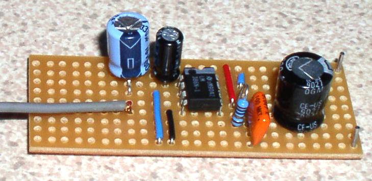
Thermistor NTC, which is in temperature contact with output power transistors, allows to separate AO LM391 power stage when it heats too much.
The standby current can be adjusted with P1. This potentiometer is initially 0 and then is adjusted to achieve a current of 50mA. Current can be increased up to 400mA if you want low distortions.
The power transistors are placed on the same side of printed circuit board, so that it can be mounted on a heatsink jointly with the thermistor. The heatsink must be large enough and have the thermal resistance of maximum 10K / W.
L1 has 20 turns with 0.8mm emailed copper, coiled over R21. C9 is a ceramic capacitor.
Guitar amp specifications
- frequency band (at 3dB/8Ω): 11Hz … 20kHz
- THD at 1kHz: 0.006% at 1W/8&Omega/Ir = 400mA
- THD at 1kHz: 0.02% at Ir = 400mA
- THD at 1kHz: 0.02% at 65W/8&Omega/Uin = 873mV
- THD at 1kHz: 0.006% at 80W/4&Omega/Uin = 700mV
Guitar amp circuit schematics

Guitar amplifier PCB layout

Simple Audio Pre-Amp circuit
Designed based on single Transistor 2N3904, this circuit will provide good gain for weak audio signals such as electret microphone. Easy to build and really simple for pre amp circuit .

14Watt Audio Amplifier + pre-amp and tone control

Use this power supply circuit:

32W Audio Amplifier Circuit based on TDA2050
Below is an amplifier Circuit based power IC TDA2050. This circuit is able to give voice to the single output of 32W with good audio quality. IC2050 can be found on the market with ease, and sold at low prices.
32W Amplifier schemitac diagrams:
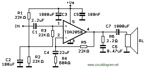
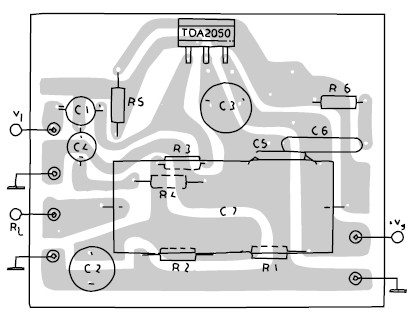
Notes:
- Use heatsinks to absorb heat in the IC
- Use recommended voltage value for maximum performance, see the datasheet.
10W Transistored Audio Amplifier circuit
Here's a circuit diagram from 10W audio amplifier. With a pair of transistors TIP41A/TIP42A main components, this amplifier audio system good enough for you because it can produce good bass with the lift curve reaches a maximum of +16.4 dB @ 50Hz.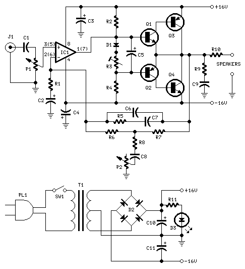 Component Parts:
P1 22K Log.Potentiometer
P2 100K Log.Potentiometer
R1 820R
R2,R4,R8 4K7
R3 500R Trimpot
R5 82K
R6,R7 47K
R9 10R
R10 R22 4W Resistor (wirewound)
D1 1N4148
IC1 NE5532
C1,C8 470nF 63V
C2,C5 100uF 25V
C3,C4 470uF 25V
C6 47pF 63V
C7 10nF 63V
C9 100nF 63V
Q1 BC547B NPN Transistor
Q2 BC557B PNP Transistor
Q3 TIP42A PNP Transistor
Q4 TIP41A NPN Transistor
J1 RCA audio input socket
Power supply parts:
R11 1K5
C10,C11 4700uF/25V
D2 100V 4A Diode bridge
D3 5mm. Red LED
T1 220V Primary, 12 + 12V Secondary 24-30VA Mains transformer
PL1 Male Mains plug
SW1 SPST Mains switch
Notes:
- Can be directly connected to CD players, tuners and tape recorders.
- Schematic shows left channel only, but C3, C4, IC1 and the power supply are common to both channels.
- Numbers in parentheses show IC1 right channel pin connections.
- A log type for P2 ensures a more linear regulation of bass-boost.
- Don't exceed 18 + 18V supply.
- Q3 and Q4 must be mounted on heatsink.
- D1 must be in thermal contact with Q1.
- Quiescent current (best measured with an Avo-meter in series with Q3 Emitter) is not critical.
- Set the volume control to the minimum and R3 to its minimum resistance.
- Power-on the circuit and adjust R3 to read a current drawing of about 20 to 25mA.
- Wait about 15 minutes, watch if the current is varying and readjust if necessary.
- A correct grounding is very important to eliminate hum and ground loops. Connect in the same point the ground sides of J1, P1, C2, C3 &C4. Connect C9 at the output ground.
- Then connect separately the input and output grounds at the power supply ground.
35W Audio Amplifier Circuit based on STK082
This is a very simple amplifier, very easy to build and produce sound output with a fairly large power of 35 watts. This Circuit used power chip STK082 as its main component. You need a split Power supply to make this circuit work. And to avoid excessive heat, you should use a heatsink on the power IC
5.8W Amplifier Circuit based IC KA2211
Here the another simple dual power amplifier circuit based on single samsung chip KA2211. This power IC only supported with a few external passive component to work and able to deliver 5.8W on each output.
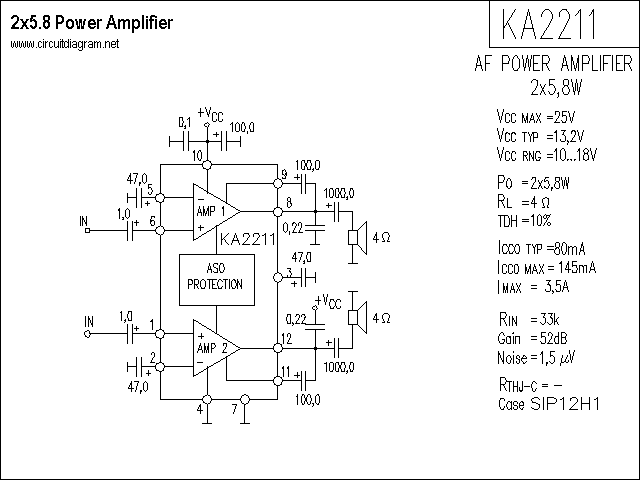
KA2211 is a dual audio power amplifier for consumer application. It is designed for high power, low dissipation dan low noise. Is also contains various of protectors and suitable for car audio power amplifier with high performance
Headphone Amplifier with LM833
This is a headphone amplifier circuit based on IC LM833 or NE5532 supporter with 4 transistors (one channel). The input can be directly connected to audio devices such as MP3/MP4 player, CD/DVD plater, radio or computer.
Amplifier part list:
P1 __________ 22K Log.Potentiometer (Dual-gang for stereo)
R1 __________ 560R
R2,R3 _______ 10K
R4 __________ 12K
R5,R6 _______ 2R2
R7 __________ 22R
C1 __________ 1uF/63V
C2,C3,C4 ____ 100uF/25V
C5 __________ 22pF/63V
C6 __________ 22uF/25V
IC1 _________ LM833 or NE5532
Q1,Q3 _______ BC337 45V 800mA NPN Transistors
Q2,Q4 _______ BC327 45V 800mA PNP Transistors
J1 __________ RCA audio input socket

Power supply part list:
R7 __________ 2K2
C7,C8 _______ 2200uF/25V
D1 __________ 100V 1A Diode bridge
D2 __________ 5mm. or 3mm. Red LED
IC2 _________ 7815 15V 1A Positive voltage regulator IC
IC3 _________ 7915 15V 1A Negative voltage regulator IC
T1 __________ 220V Primary, 15 + 15V Secondary 5VA Mains transformer
PL1 _________ Male Mains plug
SW1 _________ SPST Mains switch
Technical data:
- Output voltage: Well above 5V RMS on all loads
- Sensitivity: 250mV input for 5V RMS output
- Frequency response: Flat from 30Hz to 20KHz
- Total harmonic distortion @ 1KHz & 10KHz: Below 0.005% on 32 Ohms load and up to 4V RMS output (typical 0.003%)
- Total harmonic distortion @ 1KHz & 10KHz: Below 0.005% on 100 to 2000 Ohms load and up to 5V RMS output (typical 0.003%)
7W Stereo Audio Amplifier based LM4756
Here the another audio amplifier circuit. This is a dual output (stereo) audio amplifier based on single Power IC LM4756
15W AF Amplifier with STK075
Here the 15W amplifier based on STK075. This amplifier will deliver 12W output power.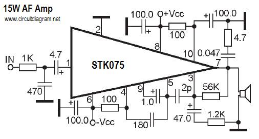
Recommended power supply voltage for this circuit is 20VDC
stk0059
![[STK0059%2055W.gif]](https://blogger.googleusercontent.com/img/b/R29vZ2xl/AVvXsEi8PM3HQmog9e_UTy6SHCSJJaxqnlps4KCfHlH2IXsPqkZw53iZ5JYdNBvTMGkmhQiQxIe_ij8GiDtE3qp4yIugAf51_mD__ny-CYfGIwY7t7A0R9Q1MGGDx5pnv4n_m3UM9DECtYqzDVU/s1600/STK0059%252055W.gif) stk006 ll
stk006 ll
![[STK0060II%2060W.gif]](https://blogger.googleusercontent.com/img/b/R29vZ2xl/AVvXsEgb_TPie94eZVl1bU9xie11ObsSgPLZxWz64eaMGXZuAUyjpPgRU6E_QUKj3ikJEGcFM_EKCRqcztxPWuQxNmEMnrMxzXED1V1ChWcQ0l0V046wMUE8ZoRctXLY-EfG5r-9F16lECEwB68/s1600/STK0060II%252060W.gif)
stk0070 ii![[STK0070II%2070W.gif]](https://blogger.googleusercontent.com/img/b/R29vZ2xl/AVvXsEggj2CA6g1tnlVNOYDn9AwYIZ6lITyQ4hB759zv8tLwPtWLZoocxOs29qNiYEKf3_0y1f3Og_vIAIPGCPBJEY3u05W0poAlP2GnO3MTcTKFxOuVQ1XZBtDdqbEjUscnlHHBaS_PXpVBYZk/s1600/STK0070II%252070W.gif) stk0080 ii
stk0080 ii
![[STK0080II%2080W.gif]](https://blogger.googleusercontent.com/img/b/R29vZ2xl/AVvXsEi5KLK2X8lHiIMeyJCFQWIXcv6Ud7KArmqtWkFTBZrMtzN9wjd2_o0dQsbfELdW6nl0EZ3j4haRCW5um0-4asjvE70ez0VGTRfDAXvSymlumdcCueWncPMGsL4G7mHSU5aPRNe8ZjFwE3M/s1600/STK0080II%252080W.gif)
stk3042![[STK3042%20UP%20TO%202X40W.gif]](https://blogger.googleusercontent.com/img/b/R29vZ2xl/AVvXsEhGCm5EvQ1-fC1wi6eJ1dIBmNAgrqVjAq0VmFfmTgc71iyzo4lBpxQWR-0NHu_ftKfkSF0EFisMTwVp0mvuOJmFfBjmiMOPcLORK6hrz_t5TjVTPxKNRP9eAoF5qmxUQ_Tjonqmv4aWcyI/s1600/STK3042%2520UP%2520TO%25202X40W.gif) stk0029
stk0029![[STK0029%2025W.gif]](https://blogger.googleusercontent.com/img/b/R29vZ2xl/AVvXsEhk8IfOkWJkUF1O6lQBHl6CHZMyrNGCi5wX06TWHyWyJXXRTFWxzcDd9TnlqLLyHDcW6Fzc12PP0QmDHFJbWWpTzu9a57wAStmOsToMyuxsiA36V7bTIseO4Xy60eSEqWwi6JvRYDWW1vw/s1600/STK0029%252025W.gif) stk0030
stk0030
![[STK0030%2030W.gif]](https://blogger.googleusercontent.com/img/b/R29vZ2xl/AVvXsEhxeV5IhGaHSbPlKsh17sv0l1sdNzdIfislytQXV42XN_17rHVCHqrDbq8y9cSqLAbpPPTVooTq1Hr8BsdvjQtVsArbrahsSLLIaJt9cQ50t0Nd1dD-vixfntSMRPDf3XCzSS6jAUFINXM/s1600/STK0030%252030W.gif)
stk0039![[STK0039%2035W.gif]](https://blogger.googleusercontent.com/img/b/R29vZ2xl/AVvXsEjXpeeGDsEeCt19E96GmjJMbG_zuuKxRPIQJT1WZIqO9E5dMevUkA4wzKDhpn0-oOCRFXAsIzl5Bwl2vg_pDHWAZa1NcxGmNGTOOW_qMziORHKjSeP3sqtZ1I3UTuc7UpA81WpMeOi6hU4/s1600/STK0039%252035W.gif)
stk0040![[STK0040%2040W.gif]](https://blogger.googleusercontent.com/img/b/R29vZ2xl/AVvXsEhMv47z8WCqNMpqtqT7cSxFbpyORIKXT2BR43W7IAgFeyivA0LSu3Bgzg75Co8wNEqR6ZFoy5aDzOKXhue67zIF-EcAnXujA4G_Vh__OkyCiJ8w-P_pcsoWegbl_-S8Bz_EI1ByvKznR9s/s1600/STK0040%252040W.gif)
stk0050 ii
![[STK0050II%2050W.gif]](https://blogger.googleusercontent.com/img/b/R29vZ2xl/AVvXsEiB-gxRzjyMA6YsOabzd1mylJtOpGaxPI-f7YUp18WtHHr7wANke7mLNbRAPKvmx6XhR7ZFEeDpjFw_OrR3B6w07VEQljBm2DCfDAjCJmTggEvmzmIkGgkC0PVokgBAQq0dKh1yI5UzhVU/s1600/STK0050II%252050W.gif)
Below is an amplifier Circuit based power IC TDA2050. This circuit is able to give voice to the single output of 32W with good audio quality. IC2050 can be found on the market with ease, and sold at low prices.
32W Amplifier schemitac diagrams:
Notes:
- Use heatsinks to absorb heat in the IC
- Use recommended voltage value for maximum performance, see the datasheet.
10W Transistored Audio Amplifier circuit
P1 22K Log.Potentiometer P2 100K Log.Potentiometer R1 820R R2,R4,R8 4K7 R3 500R Trimpot R5 82K R6,R7 47K R9 10R R10 R22 4W Resistor (wirewound) D1 1N4148 IC1 NE5532 | C1,C8 470nF 63V C2,C5 100uF 25V C3,C4 470uF 25V C6 47pF 63V C7 10nF 63V C9 100nF 63V Q1 BC547B NPN Transistor Q2 BC557B PNP Transistor Q3 TIP42A PNP Transistor Q4 TIP41A NPN Transistor J1 RCA audio input socket |
Power supply parts:
R11 1K5
C10,C11 4700uF/25V
D2 100V 4A Diode bridge
D3 5mm. Red LED
T1 220V Primary, 12 + 12V Secondary 24-30VA Mains transformer
PL1 Male Mains plug
SW1 SPST Mains switch
Notes:
- Can be directly connected to CD players, tuners and tape recorders.
- Schematic shows left channel only, but C3, C4, IC1 and the power supply are common to both channels.
- Numbers in parentheses show IC1 right channel pin connections.
- A log type for P2 ensures a more linear regulation of bass-boost.
- Don't exceed 18 + 18V supply.
- Q3 and Q4 must be mounted on heatsink.
- D1 must be in thermal contact with Q1.
- Quiescent current (best measured with an Avo-meter in series with Q3 Emitter) is not critical.
- Set the volume control to the minimum and R3 to its minimum resistance.
- Power-on the circuit and adjust R3 to read a current drawing of about 20 to 25mA.
- Wait about 15 minutes, watch if the current is varying and readjust if necessary.
- A correct grounding is very important to eliminate hum and ground loops. Connect in the same point the ground sides of J1, P1, C2, C3 &C4. Connect C9 at the output ground.
- Then connect separately the input and output grounds at the power supply ground.
35W Audio Amplifier Circuit based on STK082
5.8W Amplifier Circuit based IC KA2211
Here the another simple dual power amplifier circuit based on single samsung chip KA2211. This power IC only supported with a few external passive component to work and able to deliver 5.8W on each output.
KA2211 is a dual audio power amplifier for consumer application. It is designed for high power, low dissipation dan low noise. Is also contains various of protectors and suitable for car audio power amplifier with high performance
Headphone Amplifier with LM833
Amplifier part list:
P1 __________ 22K Log.Potentiometer (Dual-gang for stereo)
R1 __________ 560R
R2,R3 _______ 10K
R4 __________ 12K
R5,R6 _______ 2R2
R7 __________ 22R
C1 __________ 1uF/63V
C2,C3,C4 ____ 100uF/25V
C5 __________ 22pF/63V
C6 __________ 22uF/25V
IC1 _________ LM833 or NE5532
Q1,Q3 _______ BC337 45V 800mA NPN Transistors
Q2,Q4 _______ BC327 45V 800mA PNP Transistors
J1 __________ RCA audio input socket
Power supply part list:
R7 __________ 2K2
C7,C8 _______ 2200uF/25V
D1 __________ 100V 1A Diode bridge
D2 __________ 5mm. or 3mm. Red LED
IC2 _________ 7815 15V 1A Positive voltage regulator IC
IC3 _________ 7915 15V 1A Negative voltage regulator IC
T1 __________ 220V Primary, 15 + 15V Secondary 5VA Mains transformer
PL1 _________ Male Mains plug
SW1 _________ SPST Mains switch
Technical data:
- Output voltage: Well above 5V RMS on all loads
- Sensitivity: 250mV input for 5V RMS output
- Frequency response: Flat from 30Hz to 20KHz
- Total harmonic distortion @ 1KHz & 10KHz: Below 0.005% on 32 Ohms load and up to 4V RMS output (typical 0.003%)
- Total harmonic distortion @ 1KHz & 10KHz: Below 0.005% on 100 to 2000 Ohms load and up to 5V RMS output (typical 0.003%)
7W Stereo Audio Amplifier based LM4756
15W AF Amplifier with STK075
Recommended power supply voltage for this circuit is 20VDC
AN7173K
![[AN7173NK%20POW%20AMP%202X12,5W.gif]](https://blogger.googleusercontent.com/img/b/R29vZ2xl/AVvXsEiVy1mGOG7nEvqwcz49kVyx4A8wA8yyHliOP_dQi0nCbY5rnDp17V4065Ct7iY3tOncVoj6ZXit8zGtmD-Fohg0Z2A9C-_BCIntaIDC3GGq4ZKg7oytDT9W0cgU-qIIgcYa0_hhImNXoLo/s1600/AN7173NK%2520POW%2520AMP%25202X12,5W.gif)
AN7173NK
AN7168
![[AN7168%20POW%20AMP%202X5,7W.gif]](https://blogger.googleusercontent.com/img/b/R29vZ2xl/AVvXsEiEZP6-FT2PmAoT3YHFO3FeXNSrMmORgqz3cGgyATaggODEZegsQ9MoyhiPMHTMJZy3wkcUV7SoK5OE0xiUzMXflklmYnuYPGxKTnwuGjwmlhN-N80GpRbo87-nlJqcnUkPL12gH-rqblQ/s1600/AN7168%2520POW%2520AMP%25202X5,7W.gif)
AN7161N
![[AN7161N%20POW%20AMP%2023W.gif]](https://blogger.googleusercontent.com/img/b/R29vZ2xl/AVvXsEgcdCheiekbGZwrdPOI6m-W0gMeZwoSZWrS_fSEUCXWFe5F_eiIwqxNGd2IwaQnIpAH_Jt7g8iaCY036-VQpRo8d7y8QVS6hgl9ITH6QnmuvKlN-f0mgsWXKo3J5NAjhxNb-bZY4cpW8og/s1600/AN7161N%2520POW%2520AMP%252023W.gif)
AN7147![[AN7147%20POW%20AMP%202X5,5W.gif]](https://blogger.googleusercontent.com/img/b/R29vZ2xl/AVvXsEglZBFhazTAaL6hrCMTiHp2Eh723wN3HojU60fGCXmSHr3Skehjqjlilf5Oaee-yM27Dx7FQFGMYC4Tk1aOMRG-p6YVHTH8PvgF1Z6tPEhcpkkYesNxuDT7ZLiHGA3ZMnE0hzCXL9ZILq8/s1600/AN7147%2520POW%2520AMP%25202X5,5W.gif)
KA2211
![[KA2211%20AF%20POW%20AMP%202X5,8W.gif]](https://blogger.googleusercontent.com/img/b/R29vZ2xl/AVvXsEi57lcbDc4DZ6bTKnuQ0E6JVc7hh5VuK3DCubD-70BlHHhGciJLQowHwQAj1PD7hWD8_D_f7T95kPNf0aijgYU_kiUU3G0oaalQDDeBJCieFvoYOXx718xgh_6BirOt9y1aJJnuaUY7oDE/s1600/KA2211%2520AF%2520POW%2520AMP%25202X5,8W.gif)
KA2213
![[KA2213%20TAPE%20POW%20AMP%201W.gif]](https://blogger.googleusercontent.com/img/b/R29vZ2xl/AVvXsEgRIyNhcz8LLKORsVWMGD0tVO8CsYoY-u3kDoCV_zdsNf-es0L0ZAn7rMaIeF1hIKGAWIeekYjKboP_qpAPeT4QX7Hfy5WVa11Nrau-ifBNvpcPzeBLat7EhHQwEDGfaLAMhJGdnxOrDvw/s1600/KA2213%2520TAPE%2520POW%2520AMP%25201W.gif)
KA2214
![[KA2214%20POWER%20AMP%202X1,6W.gif]](https://blogger.googleusercontent.com/img/b/R29vZ2xl/AVvXsEiQ9v-rUBYei7mavtLxsB7Mor45Fw6cxxg1db72Wxi1KsCzd8tu8R98KA6JcXk3QutxgIbo1KZovSVZ6OHaPKHf_4mAIzDmJ_DIH12eVQZgrqD_SlGEzY58upgYhyzFhTae0_jAFj1Xt0g/s1600/KA2214%2520POWER%2520AMP%25202X1,6W.gif)
KA22135
![[KA22135%20PREPOW%20AMP%202X0,028W.gif]](https://blogger.googleusercontent.com/img/b/R29vZ2xl/AVvXsEi2yUOxqPo1B5GXYnxhpprXOkbk-Wec8YY_oc86ad975ONgPBo-PcDUyeBX08O9UxkCUpv3gESrEfPOv9Fn8bX1B_PY04rc2rnkPydd8X8lT6FFVnC87CjMwFjna_wFNSUa1_-9s96v12k/s1600/KA22135%2520PREPOW%2520AMP%25202X0,028W.gif)
TDA1554Q
![[TDA1554Q%204X11W.gif]](https://blogger.googleusercontent.com/img/b/R29vZ2xl/AVvXsEhv5dWFy_0iLVywFqk4uxmHpyiwTqOdEj_jPUrH_15AxUWY3dGAFfNJBik54iRSF9BpRslwU5oeBmrJ3DrkJyJPY-1MdkAkCpugS2Q4Br0IZ-jmsJfW_inRQwKRiHwCg4z_zogXksuLZ4g/s1600/TDA1554Q%25204X11W.gif)
TDA1553Q
![[TDA1553Q%202X22W.gif]](https://blogger.googleusercontent.com/img/b/R29vZ2xl/AVvXsEihc1uAVTJEzuYPt9lJKrFmZbAPKb-kFmmw1LPq_jWp5tyybJVXRHSSEhXrBxGHpOaa-cVSKGhlqNu7nvuIC4_esu8Y1001F_RwtyynffPEmQnZKEigMlsxfdqH-KMBnek2AUUKLfAuuQ8/s1600/TDA1553Q%25202X22W.gif)
TDA1521
![[TDA1521%202X12W.gif]](https://blogger.googleusercontent.com/img/b/R29vZ2xl/AVvXsEjAuHhzZ667DYhjrubpBu7KzOQXcEgW8ipy9GgOVGZryjhGXKlD4h7tBNjvcUuDQR-UhWwSgj97p5-4Eegr-UrnMOcd2tudfHc7tECbhEIGQvLvNiBwgs2L6CwaSEvST4troJktfoElsaI/s1600/TDA1521%25202X12W.gif)
TDA1514A
![[TDA1514A%2040W.gif]](https://blogger.googleusercontent.com/img/b/R29vZ2xl/AVvXsEgao4HShs1uNX2BXc9xArLKQ874ajMndV70ZWj4ic3AvreLlaJ849eEWm547VE36nLgqni7Pd0-SuSXatqQwPmxz95diFM7CMjuuev1AEHTJgGtknVOWQThACTgg4FN-BZMgJJaugG4rKU/s1600/TDA1514A%252040W.gif)
TDA1010A
![[TDA1010A%209W.gif]](https://blogger.googleusercontent.com/img/b/R29vZ2xl/AVvXsEhom8btof0nQUQWXFetrgMAaC1EubNLOxARB-lD3BX9xzJPGciFz_ICJG-sVrsMdZX_rD-OI910szzJ7Vkuxtubnel_q-VBQz9VKJymYR4ZMjubtHnQuIjslnriwJecatayCwAUCIv1ets/s1600/TDA1010A%25209W.gif)
TDA2040
![[TDA2040%20HI-FI%20AUDIO%2020W.gif]](https://blogger.googleusercontent.com/img/b/R29vZ2xl/AVvXsEgln_dvZEahdg9SguMBofrnnVNy-mINEAMUYmdOCEk4eTSZw08iQhQzOgp6lbtPmjDBrn2tDNm3g4q0Km3ar0hwXbqWjIh1iXilwxRndgalR6eEHUT-YK_Ec3n7S38BFnZnHxc1wIesP-k/s1600/TDA2040%2520HI-FI%2520AUDIO%252020W.gif)
TDA2008
![[TDA2008%2012W.gif]](https://blogger.googleusercontent.com/img/b/R29vZ2xl/AVvXsEjCb1vKbFqLitMlJlxI9_m83BLy3tam7T35eTL2ZVXsuZ4z01T3RCkGXIQadewUK8r_LjfzkWh8EWwLHY6DKd3aFt81KjymuFUZvyiyVHZALQNvblfnDQaSj83559rOvCVnox1pFjOIE20/s1600/TDA2008%252012W.gif)
TDA2004
![[TDA2004%202X10W.gif]](https://blogger.googleusercontent.com/img/b/R29vZ2xl/AVvXsEj0U2590yQG1p5yYzl8Lw96kYSjKzF8lTKm0VRdV1vrVQVLnV2bkbWq2RQaF-3H3pmIzrHVP38b3cibqk5Uw-8c9mgDXHAN_k1_fZyT3o9tcUDX3a_hr_76YzDLnVoI2i4zRCgULag_XEE/s1600/TDA2004%25202X10W.gif)
TDA7350
![[TDA7350%202X12W.gif]](https://blogger.googleusercontent.com/img/b/R29vZ2xl/AVvXsEgjopHpJ1beHgWTVGdQT9zNgR5qABQJ_8uxf-n5UG_D8RFSk2XV3dYT3jSzfIT-63qh6-JBnRH5wtYVreaotQ8oegyGXlBoBxDAJBTdFZCX0qgK7-igm6nsLCTI2TUKit-Cq1PKV2bhe8Y/s1600/TDA7350%25202X12W.gif)
TDA2003
![[TDA2003%2010W.gif]](https://blogger.googleusercontent.com/img/b/R29vZ2xl/AVvXsEjtb6sqi_rj8P7ZjPJFiX8-SH3fre-BA9im5pxCSZR0N107j327r19LaWzYHtj2czr10GqNqqha1b-yJjF3Gkow2Hjh44fOd7Mun36z6WnAEk9wj2F1qEeCOqmLjFydBtfu-iDoIWEsIEg/s1600/TDA2003%252010W.gif)
TDA7241
![[TDA7241%2020W.gif]](https://blogger.googleusercontent.com/img/b/R29vZ2xl/AVvXsEhaS8mWEJhWDnPrOnpAGwmuJrMi8hLYmhf1F0ZS3kgie79LI7aFNVPgFvyTsh6Vd5Pm6Rq73qHwxZ0NMFJLlBqBYYw-q1GtSiOuodJ5NOX2tI0gpy_Vur7udJfikt9cGizoqtGdVQp54FY/s1600/TDA7241%252020W.gif)
TDA7233S
![[TDA7233S%2016W.gif]](https://blogger.googleusercontent.com/img/b/R29vZ2xl/AVvXsEjbDGIHeSvA2UJmtffn-Oa4fRLbzAIj5WHJevCI5i44KHCTSgzmcQdDAtbWQFsmzGx7qp1JM5MfJgqxKU-kvWW8_YPuKiZG86pt7VqkilM9E3M13kFldgn50owBU-6iZl8Xkc-kkTLILhw/s1600/TDA7233S%252016W.gif)
TDA7057Q
![[TDA7057Q%202X3W.gif]](https://blogger.googleusercontent.com/img/b/R29vZ2xl/AVvXsEheA4sUxp7_7p6gmJMKHKJ70rl4NL9pCFD-OMXu52AvOp3O6oxrxP5ZYAJ9tTf7aDRoaKV69yF_L8rJgaQDAKzVrxcthzJNhgnj4cq9skDW4CFUAWdoONQkCEK-mlQiv9vQAudE4SyHYiY/s1600/TDA7057Q%25202X3W.gif)
TDA2040
![[TDA2040%20HI-FI%20AUDIO%2020W.gif]](https://blogger.googleusercontent.com/img/b/R29vZ2xl/AVvXsEjUK2amYOZRJHoJB064cB7APjwN_1BIdE5K-Q2Vb8dLJSNR_e-9nNf_j1ExaY6XZ5CRnUKKaiEeqnbuW4GTlbz9q5xVwql9ynWhrrEkaYvkslzj1GYperzxztJgoPKuT5Ap6GsJJLWxxdo/s1600/TDA2040%2520HI-FI%2520AUDIO%252020W.gif)
TA7250P
![[TA7250P%2023W.gif]](https://blogger.googleusercontent.com/img/b/R29vZ2xl/AVvXsEh9JnwAaXy8A2U5KTigRRSZPbHE8e2W8f8-p0aVKSMO_acIucuWuSO-kOLv4wT5_x9mlx0J2Jg0a5JTWfVWuQ59VVCBw5x19rtN9w8_6I9XlzDb9EbJbQKE2oVb7B57DGh8ao_WcLr4-jo/s1600/TA7250P%252023W.gif)
TA7273P
![[TA7273P.gif]](https://blogger.googleusercontent.com/img/b/R29vZ2xl/AVvXsEidN3T-R1zuzCuvMYk79gRNiDBQjKLD7M1tvT_pVdU-QV6fFp-b-SP1oMbdGpCGUmluTfUrmZkwfRJHAZD1vO0mW9zgUn3Ylhk4Wwnnuc-ijMa1I5hI4aa6weq7xaAYNxJdm95dufJwzBs/s1600/TA7273P.gif)
TA7240AP
![[TA7240AP.gif]](https://blogger.googleusercontent.com/img/b/R29vZ2xl/AVvXsEiuFj-Th0x7X-0ocJga7qwXXUqAJ_M90RkCnFglqoIQtHi7FFwTtsfnRmB8OOkdzh57NrE0b62uhyphenhyphenUfxDRPgQWrsouwnVbWxbLcGFfcgfrsb5iwO940E9JeWxMCIDtyqkSpnfEXEbku93Q/s1600/TA7240AP.gif)
TA8211AH
![[TA8211AH.gif]](https://blogger.googleusercontent.com/img/b/R29vZ2xl/AVvXsEgRjhMIHPHYaGCBcuGwehjAmCRDivvzDO47IAL5WK279K6auhEFa80UG8uwFuLskBsk5GdikW34rGpZZsFoA4ixXrIeZw4yeCJRpwMYeaSnx-K58BwhWIocpg6TyZJ8hWB2oCV1M5AeXs4/s1600/TA8211AH.gif)
TA8200AH
![[TA8200AH.gif]](https://blogger.googleusercontent.com/img/b/R29vZ2xl/AVvXsEiFkYXiItqAZh8mC8t-83AHoeQqLpuSQP9fIq6FuWUkzvzIIUGgprS0u4a_5oZSawN9RgVEeeuVT3NMCZrfDxAVfrsFS2I-ka-Y_dWBcXkiDeBf3myjve2n2y9zD8BGtOI7OVqHVqq0QO4/s1600/TA8200AH.gif)
200W POWER AMP
number name
Transistors
12x Q1, Q2, Q5, Q7, Q9, Q10 MPSA 06
10x Q3, Q4, Q6, Q8, Q11 MPSA 56
4x Q13, Q14 2N 3439
4x Q12, Q15 2N 5416
2x Q16 MJE 15030
2x Q17 MJE 15031
4x Q18, Q20 MJ 15003
4x Q19, Q21 MJ 15004
Diodes
12x D1, D2, D3, D4, D11, D12 1N4007
12x D5, D6, D7, D8, D9, D10 1N4148
8x (15x) D13, D14, D15, D16 20 V Zener +5% tolerance, 0.5W
Capacitors
2x C1 390 pF mica
14x C2, C3, C15, C16, C23, C24, C25 100nF/100V film
8x C7, C12, C17, C18 100nF/50V film
12x C4, C5, C13, C14, C21, C22 100uF/63V radial electrolytic
2x (4x) C6a, C6b 220uF/16V bi-polar electrolytic (4x 330uF/16V)
2x C8 180pF mica
2x C9 47pF mica
4x C10, C11 10pF mica
4x C19, C20 10nF/50V film
Rezistors
All resistors are 1% carbonic or metalised 0,5W if not noted otherwise
2x R1 20 kohm
2x R2 2 kohm
16x R3, R4, R5, R6, R7, R8, R9, R10 300 ohm
6x R11, R12, R27 1.2 kohm
4x R13, R14 2.2 kohm
4x R15, R16 12 kohm
4x R17, R18 11 kohm
2x R19 1.1 kohm
2x R20 22 kohm
4x R21, R22 30 ohm
4x R23, R24 360 ohm
4x R25, R26 1 kohm
4x R28, R29 270 ohm
4x R30, R31 3.9 kohm 1/2 W
6x R32, R33, R51 82 ohm
4x R34, R35 330 ohm
2x R36 220 ohm
8x R37, R38, R39, R40 680 ohm
8x R41, R42, R43, R44 10 ohm 1/2 W
8x R45, R46, R47, R48 0.33 ohm 5 W wire-wound
4x R49, R50 10 ohm, 2 W
Other
2x P1 2 kohm more turn cermet trimmer
1x T1 Toroid power transformer SEC 2x40V AC 300W
8x C1P, C2P 4700uF/63V (6x 6800uF/63V)
8x C3P 100nF/200V
1x D1P Bridge rectifier 35A/200V
5x
Fuse casing
1x F1 Fuse 3.15A T
4x F2, F3, F4, F5 Fuse 5A F
8x
Insulative bed under transistors + screw insulatives 16x
20x
Solder eye M4
2m
Shrinking spaghetti 4mm
160 WAP STA5150
![[Graphic2.jpg]](https://blogger.googleusercontent.com/img/b/R29vZ2xl/AVvXsEgMnBSv15TmRAXJa78cbRgplGK67CuGszUiM5rEMcydyJQTUq05xHH2No6M97TE4HroPa8-vtQwYWiplB_APnmm0AK6YMfZ0w5hUI6DmxRmbOGYshSubjPN_v_PW-lIbmX9yz6WcIWsD7w/s1600/Graphic2.jpg)
![[Graphic1.jpg]](https://blogger.googleusercontent.com/img/b/R29vZ2xl/AVvXsEgkmh0IMc9yW3zvXb_hwF3umk8MsAyh_bIglA-nADTi1U_7NBSCLQpoLwp8qt2e0jSWwnDQukHc63YLEkP897T9C6YoPWfppK_94MSToUjsGJ3ICNrQxcM3dMwShFllfS1Rtrzwb5ST6zo/s1600/Graphic1.jpg)
![[Graphic4.jpg]](https://blogger.googleusercontent.com/img/b/R29vZ2xl/AVvXsEhVNW7DFUSu1cO9t2q0rdRM0AaaMflvpDYl3khlt7sClVeul46zC6gKMCjPN5Q4jCIU7fggyiGndQvwX1dErjpaiRanmv-IedH8JUXAJV_uFVK7eglkoFT0aMhK5FGmy2rU4bKIQ2rOq_A/s1600/Graphic4.jpg)
![[COMPONEN.jpg]](https://blogger.googleusercontent.com/img/b/R29vZ2xl/AVvXsEgMuIcWWF98Y9Lco6uVR_KllNISHaszg6U-j0Ta-trwMsTwpcGLlTaikIfcXc36p30Hj1B8ye83uTUv9XqPBb5Vcu16iyBFhDbOjuDjv9DwglOxZV0js6csQadxHxWQFFxEQdkTtTgVKzo/s1600/COMPONEN.jpg)
![[SPEC.jpg]](https://blogger.googleusercontent.com/img/b/R29vZ2xl/AVvXsEjAqJwNLiJKa-C629DwrUIITOah_3c3O1xArBCbY4d4JtSQPWknxIRVDgRtGVF7N2IPqEKbyzXz3nNJF8ZgQDa-Hbk5G5ys9ez123T5NlZ0nvfp2L4RejwdaBkhdpkf7tBoUorBmFUzPyg/s1600/SPEC.jpg)
150W MP3 CAR AMP
![[mp3+player.jpg]](https://blogger.googleusercontent.com/img/b/R29vZ2xl/AVvXsEgN6m3Jix2Q5Vg3i7jo8T6tCjqLzdpNdvz5_f6jaGPtiSCYF2uq5hzaCgQ3BKx4EcEPjkP481BSpTUvu1mnlnnTAW1jAfQpr2dQSw5ZJ_hqgPyR8v0w2wPAzkxWfgcQiPUzFn8ir0xOdwM/s1600/mp3+player.jpg)
![[preampli2.gif]](https://blogger.googleusercontent.com/img/b/R29vZ2xl/AVvXsEjENorI5rVSkhyiq4fwaj7dvJOwXQDuHBEuZ6VUKc6BBi7-6o-GCXI038QSsAmRTUU3roz1Sl_VdFGUDJ7t2I8wHWa84QOIdYVP8_XHSn-HppP8OMdFkYc4qrFnm46FbocfykYSxDF2ZFo/s1600/preampli2.gif)
Description :
LF353 Wide Bandwidth Dual JFET Input Operational Amplifier
General Description
These devices are low cost, high speed, dual JFET input operational amplifiers with an internally trimmed input offset voltage (BI-FET II technology). They require low supply current yet maintain a large gain band width product and fast slew rate. In addition, well matched high voltage JFET input devices provide very low input bias and offset currents. The LF353 is pin compatible with the standard LM1558 allowing designers to immediately upgrade e the overall performance of existing LM1558 and LM358 designs. These amplifiers may be used in applications such as high speed integrators, fast D/A converters, sample and hold circuits and many other circuits requiring low input offset voltage, low input bias current, high input impedance, high slew rate and wide bandwidth. The devices also exhibit low noise and offset voltage drift. (National Semiconductor)
Features :
Internally trimmed offset voltage: 10 mV
Low input bias current: 50pA
Low input noise voltage: 25 nV
Low input noise current: 0.01 pA
Wide gain bandwidth: 4 MHz
High slew rate: 13 V/us
Low supply current: 3.6 m
High input impedance: 1012.
Low total harmonic distortion : <>
Low 1/f noise corner: 50 Hz
Fast settling time to 0.01%: 2 us
![[powerpng2.GIF]](https://blogger.googleusercontent.com/img/b/R29vZ2xl/AVvXsEiTzpY5H9XCwawMSiLLSiM69RJxppOUdvg-bsl7-hkFYp3OVX88VFwTYbK6XXM0_m31tU4DbzFauIUGJNADrIHj2fpVrVY9ABCoOzgv8_TkWkFpAvIWQ9prrV89qNC9GdhJDz_6TarP_VI/s1600/powerpng2.GIF)
LA47536 Four-Channel 45 W BTL Car Audio Power Amplifier
The LA47536 is a 4-channel BTL power amplifier IC developed for use in car audio systems. The output stage features
- A pure complimentary structure that uses V-PNP transistors on the high side and NPN transistors on the low side to provide high power and superb audio quality.
- The LA47536 includes almost all the functions required for car audio use, including a standby switch, a muting function, and each protection circuit. It also provides a self-diagnosis function (output offset detection). (Sanyo)
Functional Description
1. Standby Switch Function (pin 4)
The pin 4 threshold voltage is set to be 2 VBE. When Vst is 2.0V or higher, the amplifier will be on, and when Vst, is 0.7V or lower, the amplifier will be off. Note that pin 4 requires an operating current of at least 40uA.
2. Muting Function
The IC is set to the muted state by setting pin 22 to the ground potential. In this state, the audio output is muted. The time constant with which the muting function operates is set by an external RC circuit, and this time constant influences the pop noise that occurs when the amplifier is turned on or off.
The muting on and off times due to the recommended external component values (R=10k, C=3.3uF) are as follows.
Muting on time: 50ms
Muting off time: 20ms
3. Self-Diagnosis Function (Speaker burnout prevention)
During steady state operation, the LA47536 detects, internally, whether or not an abnormal amplifier output offset has occurred, and outputs this signal from pin 25. Applications can prevent speaker burnout and other problems by having the system microcontroller detect this pin 25 output signal and control either the standby state or the power supply. (An abnormal output offset may be caused by, for example, input capacitor leakage current.) The pin 25 signal is turned off by setting pin 1 to the ground potential.
4. Oscillator Stability
In some cases, parasitic oscillations may be induced by the PCB layout. This oscillation can be eliminated by adding the components listed below. Note that the optimal capacitor value must be verified by testing in the actual mounted state in the end product. Connect a capacitor and resistor (0.1uF and 2.2) in series between each output pin and ground.
5. Audio Quality (Low band)
The frequency characteristics in the low frequencies can be improved by making the capacitance of the input capacitors variable. The recommended capacitance is 2.2uF and smaller.
6. Protection Circuits
Do not ground the outputs with the STBY voltage at around 1.4V. Also, do not turn the IC off in the grounded state with a time constant provided for the STBY voltage.
7. Pop Noise
Although the LA47536 includes an pop noise prevention circuit, pop noise can be reduced even further by using the muting function as well. Activate the muting function at the same time as power is applied. Then, after the output DC potential has stabilized, turn off the muting function. When turning the amplifier off, first turn on the muting function and then turn off the power supply. These two methods are effective at minimizing pop noise.
![[preamplipcb3.GIF]](https://blogger.googleusercontent.com/img/b/R29vZ2xl/AVvXsEgLtt-7zsSbZci93LJeBD943sLu1ozI-ZmFoc8v1AqU0ldmA047zkcEBCdbC0zO_PKB2aefjSCJDn-JimEglm96J_82eqhwvBbviajSX2Ecrfp0T96KVTxSfXuuaW20Zs3laFPUZ0W1pkQ/s1600/preamplipcb3.GIF)
![[pcb2.gif]](https://blogger.googleusercontent.com/img/b/R29vZ2xl/AVvXsEjdCdwFc9Y1QbqYGZQwmfKDggIMwBGYJzEhmYmVFacLODAo1W_lkve2HPVpoL3Mi4UBJ6Y_UlI50wl4jU-g5IhQFKL-Sc_FLuyQyf4nkrcYvvkugW9hePP4zbTxzcS8TPtUXW7r7j3-2TE/s1600/pcb2.gif)
HIFI POWER AMPLIFIER
DESCRIPTION
Characteristic Summary : power amplifier mosfet complementary symmetrical hifi complete with very height output
power and good dynamic, because real delay of the way in level of end exploited for
compensation of frequency to be obtained absolute stability
Output Power : 140 watt at 8 ohm each chanel / 180 watt maximum at 8 ohm
180 watt at 4 ohm each chanel / 250 watt maximum at 4 ohm
Distortion : less than 0,01 % at 140 watt and 8 ohm / at 180 watt and 4 ohm
Input Sensitivity : 1 volt-ef for 130 watt at 8 ohm
Input Impedance : 25 Kilo-ohm
Frequency Characteristic : 4 - 50000 Hz (with source resistance 600 ohm)
![[BLOK+SKEMA.jpg]](https://blogger.googleusercontent.com/img/b/R29vZ2xl/AVvXsEjK-krEu72x-hX8MCT_ISqC8NbyvRzEN4JB-rt9d_LHWcSDPSk6ybPZKLs1Fv_ZKkYf5ghF4LznJILTqmhyphenhyphenhpNiWuhTCEjb-PKJgNWXjj_iUwX1qOe41R-Vl4xdCY6sB6964xhYfJvCyNo/s1600/BLOK+SKEMA.jpg)
![[CATU+DAYA.jpg]](https://blogger.googleusercontent.com/img/b/R29vZ2xl/AVvXsEjz_-JwlQ9ly35w89iGDXtJdB4xpx70E2vGVp8m5jyCdjtjjY-pBff0XNlgAUdUS69TA7R3B5zsA2qRsZ-uelDhcZkngGVQ_yR6IRYDrblhpcTzKmOZ7rr50nmTbORBR7LJkzyN3HZVBqw/s1600/CATU+DAYA.jpg)
![[SKEMA+MOSFET.jpg]](https://blogger.googleusercontent.com/img/b/R29vZ2xl/AVvXsEjxbEPQ9Iddc09WwJ4f7SkQhqPBRKN5U3fOhDw1XXaCD8xfT-cBePJVv8GyjWkH4d_6xmuNRGsjGCrqHe3Sbcqp5a3GG33yZB_zuEgMP1lL1ZJxJi3NM6RZKk12OEnRjzQl8LsUJ02jfLc/s1600/SKEMA+MOSFET.jpg)
![[DAFTAR+KOMPONEN.jpg]](https://blogger.googleusercontent.com/img/b/R29vZ2xl/AVvXsEipQpvGNvhjEI9OEzN5ZMc_b6aBHJue8k5vjOyK6rNOEOKyZo1-9UXsLp1G_khJjPRUJ5IJQjXi78c2943b8aPi-4OQ3Gt7cn0MtyofAXhkqZbA9IyocKh0CyQ9Ckta6yGwpUdgFQrKhRY/s1600/DAFTAR+KOMPONEN.jpg)
![[pcb+bawah.jpg]](https://blogger.googleusercontent.com/img/b/R29vZ2xl/AVvXsEhApfDDsCN7aXWpYlE3L1DxXYaCYfJHoPRkixs7g7lwEtZYhj9F6vN-0fLV3Pd7Q-KTF5N-ZHZmOXhcl6ZyeBG3UV3h7PnKGN1U1gzk9zivyyd7CBORAtA0MqqCunyoPeWhSpFYlR9msTk/s1600/pcb+bawah.jpg)
![[pcb+atas3.jpg]](https://blogger.googleusercontent.com/img/b/R29vZ2xl/AVvXsEimRX6UEBhMpB_yJ7IwcvwUMbk1EPLxbIx7mqrwFfsfdNh2Q6-WytnKXaH_d4oK6bRQlVcc00k8SMNCAUI6jhU97RV62cglR0-HnB0_HCNYsTwVN_ZE43RfrmSLuC9XJasvIXFIU198JQE/s1600/pcb+atas3.jpg)
POWER AMPLIFIER (TDA7294)
![[tda7294+pin+conection.jpg]](https://blogger.googleusercontent.com/img/b/R29vZ2xl/AVvXsEh4QC42rqswLaev2YNMFsa6PjtgNhXqWMYJOzY5Bf3ZVx44BhbAdahyRGYIFyL1n_4zLrzXwBdy1TbJvULVXhm-qaqQhqilyctt_Q0gyJzB0cGzMLNYQRt-uLECloPi4oPzSHSE9keMXK8/s1600/tda7294+pin+conection.jpg)
![[tda7294+body.jpg]](https://blogger.googleusercontent.com/img/b/R29vZ2xl/AVvXsEh9_5-nNirS6ILZwuoraJbtIIlqQzirqaD2ZAWW7pjDwH-ZsKXVHhdiQP19YLlI6kPOQc9pS_0G5te-UBonheIsVce60rp0j_LIMjpNPiIc7I6FoTHKetrueNbqDDKdsNahCPxC1ZQ5dgI/s1600/tda7294+body.jpg)
![[tda7294.jpg]](https://blogger.googleusercontent.com/img/b/R29vZ2xl/AVvXsEjBhgj5F8-sunXPDoZcLj5JhvwdNQMNOPv7xkvj_h5fXDXvbqK5l62W8bwtoKwJRNRNn7tmNyd7I5w6xJxnBKi8__n149bSWLTZ4ckPRBppaOCo7zbZ-NTG-EmhPhvNFWSpYdXIlImLWI8/s1600/tda7294.jpg)
ELECTRICAL CHARACTERISTIC (Refer to the test Circuit)
Vs = -35V, RL = 8W, GV = 30db,
Rg = 50W, Tamb = 25ºC, F=1kHz
| Audio Circuits |
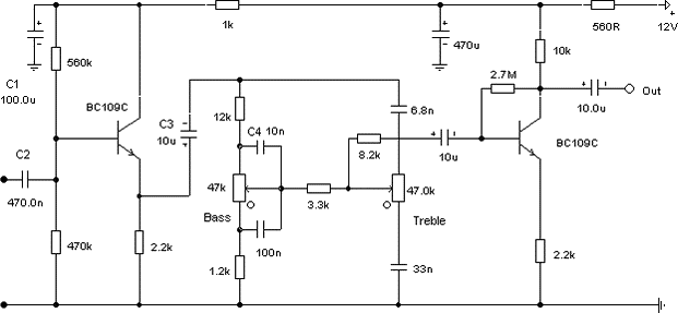
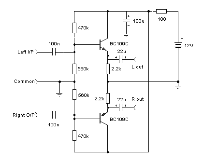
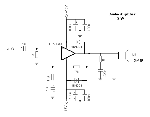
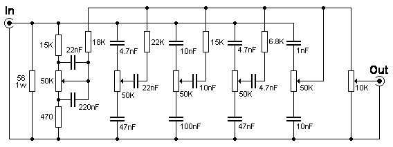
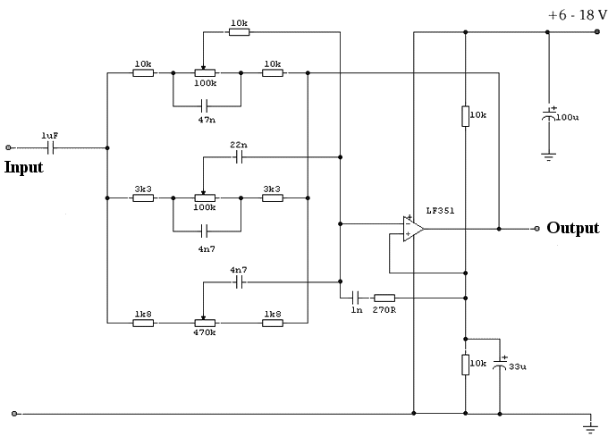
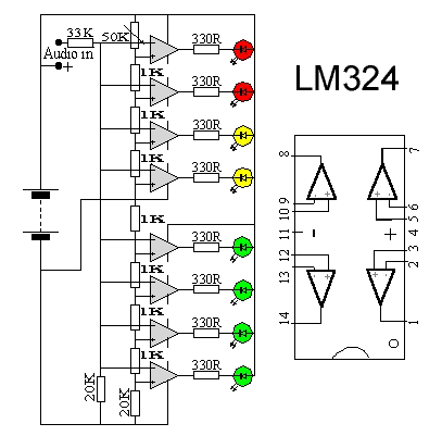
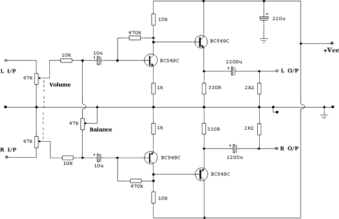
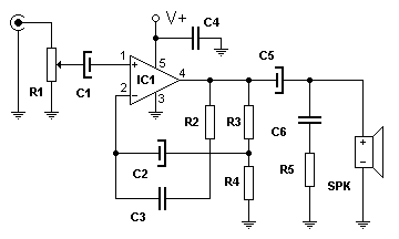
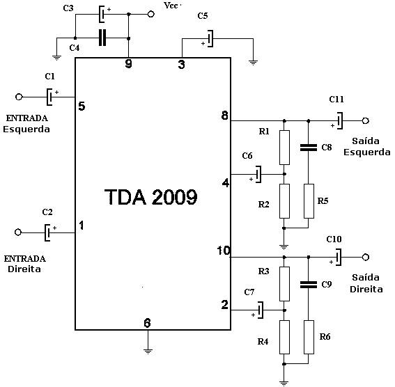
Amplificador 100W
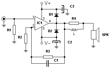
O amplificador em si é o circuito integrado LM12CLK que é um amplificador operacional de potência.Permite debitar na saída com uma impedância de 2 Ω , 150W de potência. Por segurança e estabilidade optamos por fazer o circuito para funcionar com impedâncias de 4 Ω onde obtemos uma potência RMS de 100W.
A bobina L na saída é formada por 14 voltas fio nº 18 com núcleo de ar de 1 polegada.
A resistência de 1.1 kΩ deve ser de precisão. A resistência de saída (em paralelo com a bobina) deve ser de 2W de potência.
Os condensadores electrolíticos devem ser de 50V ou 63V.
Alimentação :
- V max: simétricos +/- 24V DC
- I max: 5A
Componentes:
| R1 1 kΩ | C1 2.7 nF | D1 6A2 | ||||||||||||||||||||||||||||||||||||||||||||||||||||||||||||||||||||||||||||||||||||||||||||||||||||||||||||||||||||
| R2 1.1 kΩ | C2 4700 µF | D2 6A2 | ||||||||||||||||||||||||||||||||||||||||||||||||||||||||||||||||||||||||||||||||||||||||||||||||||||||||||||||||||||
| R3 3.3 kΩ | C3 4700 µF | IC1 LM12CLK | ||||||||||||||||||||||||||||||||||||||||||||||||||||||||||||||||||||||||||||||||||||||||||||||||||||||||||||||||||||
| R4 2.2 Ω Audio Amplificador 50 W 
| SPK alt. |